ATTINY 44
The Data sheet for the ATTiny44 can be found HERE.
The ATTiny 44 is an 8bit AVR microcontroller. It has:
---> 32 x 8bit registers ---> 2k (t24) / 4k (t24) / 8k (t84) of Flash Memory. This is where programs are stored.
---> 128 (t24) / s456 (t44) / 512 (t84) bytes of SRAM. This is used to hold the data that is processed during runtime.
--->128 (t24) / s456 (t44) / 512 (t84) of EEPROM which is data that is stored but can also be changed.
There are 12 data pins on the ATTiny 44.
---> 8 x PORTA Pins. Can be input or output, also have analog to digital converters (ADC)
---> 4 x PORTB Pins. Can be programmed as input or output also have special functions
---> Special pins on PORTB include: CLKI on PB0 for external clock in // XTAL on PB1 for manipulation of an internal oscillator // RESET on PB3 to reset programs and perfrom timing functions // and CLKO on PB2 to output system clock data.

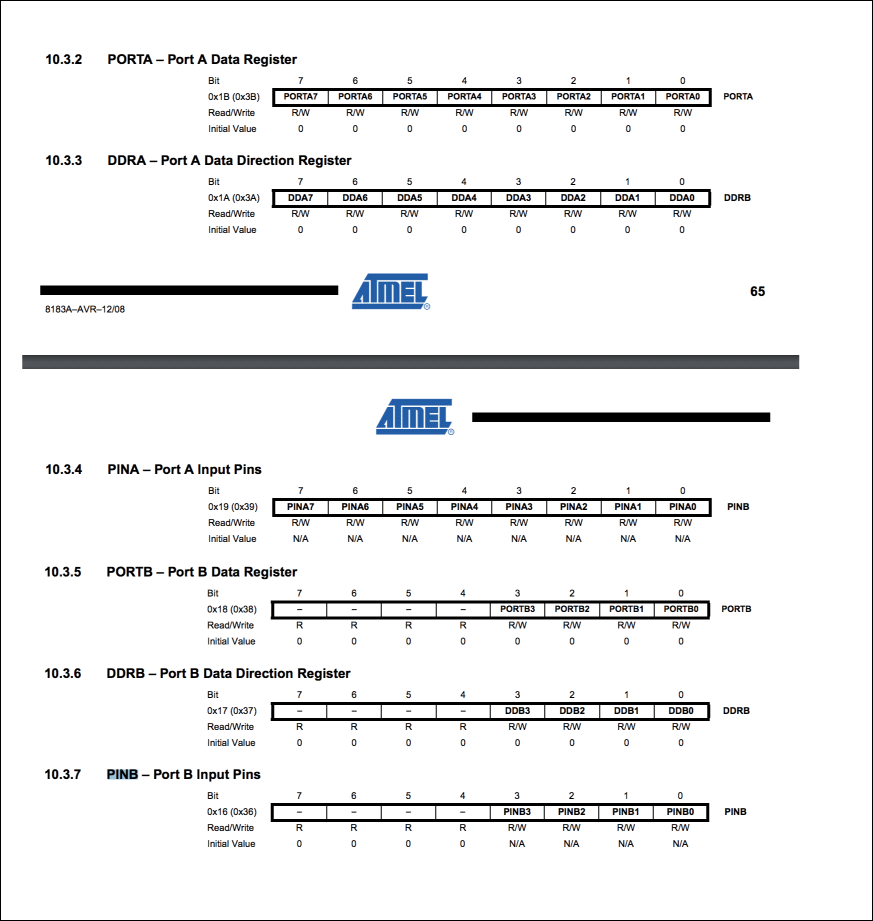
The following pages from the ATTiny data sheet (pages 65 & 66) represent the bit registers on the ATTiny. Each port has three registers DDR, PORT, and PIN. Smaller chips like the ATTiny45 only have one port. Understanding what the three registers do is helpful if not necessary when setting up your code outside the Arduino IDE environment.
---> DDR: Data Direction Register. Decides whether a pin is an INPUT or an OUTPUT. When set to 0: pin is set as n OUTPUT. When set to 1: pin is set as INPUT.
---> PORT: An Output register that is used to set the output value on a pin HIGH or LOW 1 or 0 (5v or 0). It can also be used to set a pull-up or pull-down to cancel noise on an input.
---> PIN: Input register used to read the voltage at the pin.
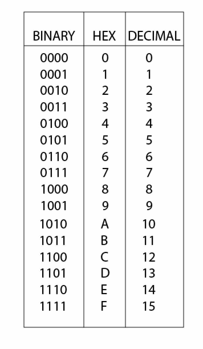
Understanding registers and how to switch them is important but somewhat cryptic. Below is an example of Logo code that Brian Silverman showed me to turn a light on and off. I was completely confused until I drew it out. I learned 2 things about binary. One is to use it as a map to locate the setiings on a particular register. The second thing I learned is to use it as a value in itself. In this little bit code we are using decimals to represent the locations on the register that we need to set. You need the datasheet to understand it.
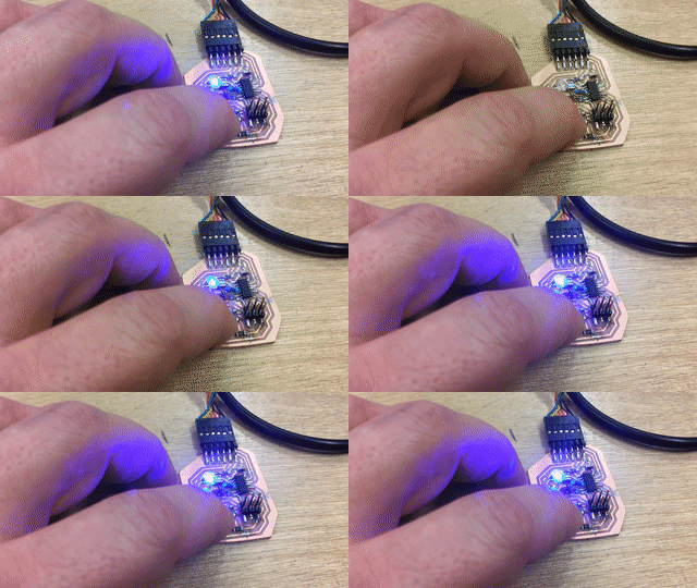
What I needed to do was to figure out which pins on the ATTiny were setup as outputs so that we know how to make our blink code and to turn an LED that was attached to PA7 on and off. Here is the code that tells us which pin is an output and how we can turn that pin on and off:
prhb readb ddra
82
bsetb porta $80
bclrb porta $80
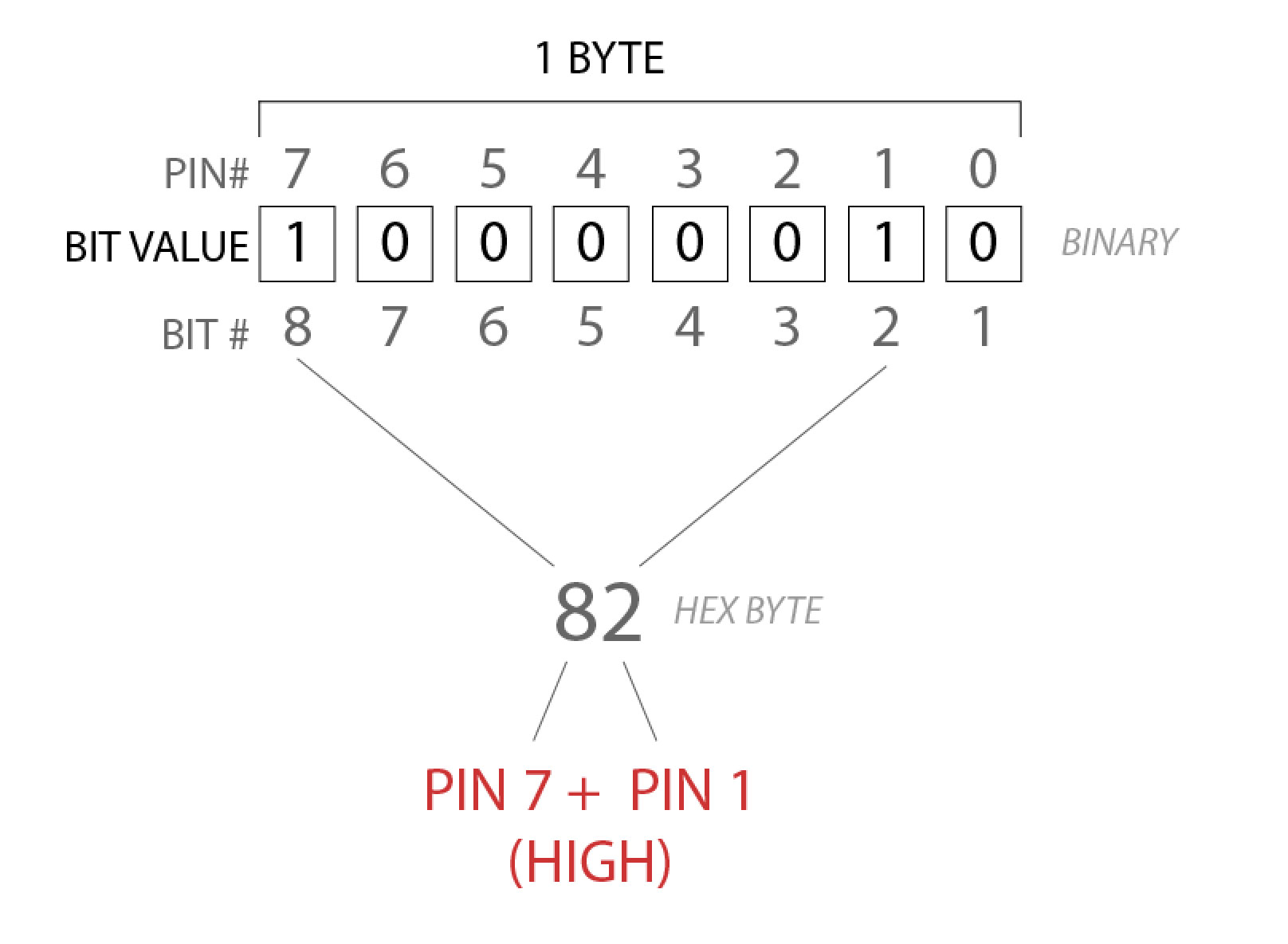
First thing that really confused me was remembering that 8 = 7 and 2 = 1 in the register. The second is to remember that we read from right to left.
What the above code means is:
---> prhb = print as a hex byte
---> readb = read the byte value
---> ddra = data direction register on port A
In english, reading right to left, this says: On the data direction register for port A, read the byte value, print it as a hex byte. The return was 82 which means that in the DDR register in PORT A PA7 and PA1 are set to HIGH making them OUTPUT pins.
Remembering that 82 is a map, it tells me the location on the Data Direction Register. Here is a diagram I made to help me visualize this:
To understand how the binary relates to a HEX or DECIMAL type:
To turn the LED on and off:
---> bsetb porta $80 = set a bit on pin7 in the PORTA register. It will go from 0 >> 1 = HIGH
---> bclrb porta $80 = clear the bit on pin7 in the PORTA register so it will go from 1 >> 0 = LOW.
For the register on PORTA this looks like 10000000. The only place where $80 is adressing is PA7.
