Board Design with Kicad
To design the electronics for this week, I have decided to design the board using Kicad. Kicad is open source electronics design program that has a wide variety of libraries to install. I downloaded Kicad and then attempted to clone the symbols and footprints. Cloning them through Git Bash was not successful and so I downloaded them regularly through their websites. Once the download is done, I followed these series of steps.
Pick the hello-world board that you would like to design and produce.
I picked the ISP ATtiny 44 board. The reason for that is that I still have not been able to wrap my head around the concept of the electronics and their logic. For that reason, I felt that this board is very simple to design and produce.
Find the necessary components
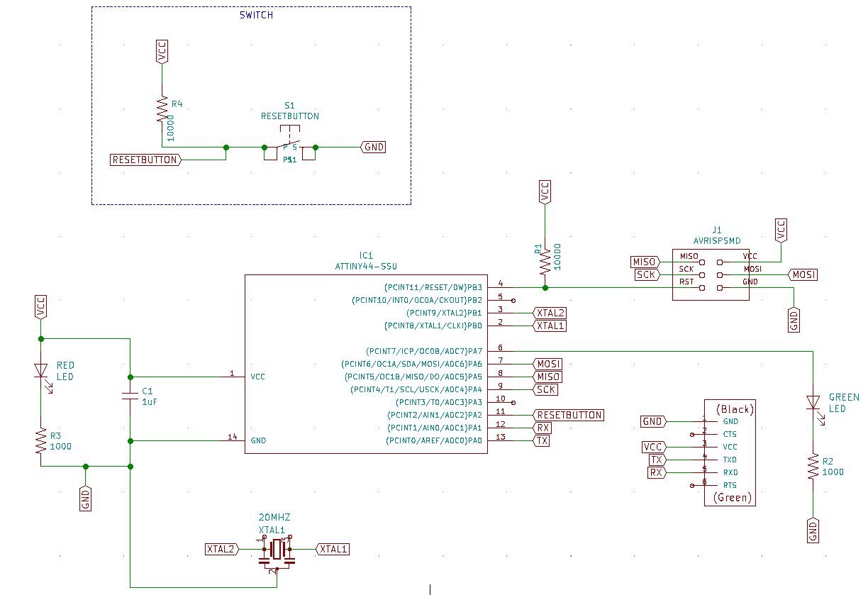
Looking through the components list provided and board images, I was able to find the necessary components. The components are: - ATtiny 44
- Resonator
- 6MM Switch
- AVRSPIMD
- Green and Red LEDs
- FTDI-SMD
- Capacitor, 1uF
- 2 1000ohm and 2 10000ohm resistors
Open Eschema, add components, and connect them
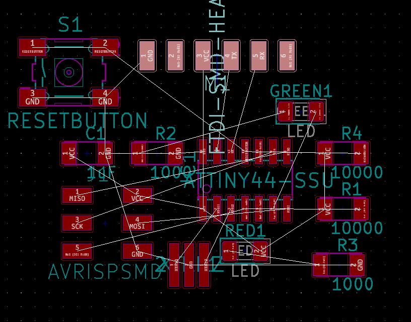
Open up the Eschema editor "schematic layout editor" which is the first one of the 8 horizontal symbols, and once the eschema window opens, select the "place symbol" which is the third vertical symbol on the right, then click on anywhere on the screen and search for the necessary components one by one. Once all the components are placed in the window, you can beging to move them and rotate them to look how you would like them to connect. To make it easier for future reference, you can hover over a symbol and click on "e" where you can edit the name of each component. Another important information to remember is that you can connect different symbols like voltage or ground virtually by placing labels with the same name. The program understands that they are equivalent.
Check footprints
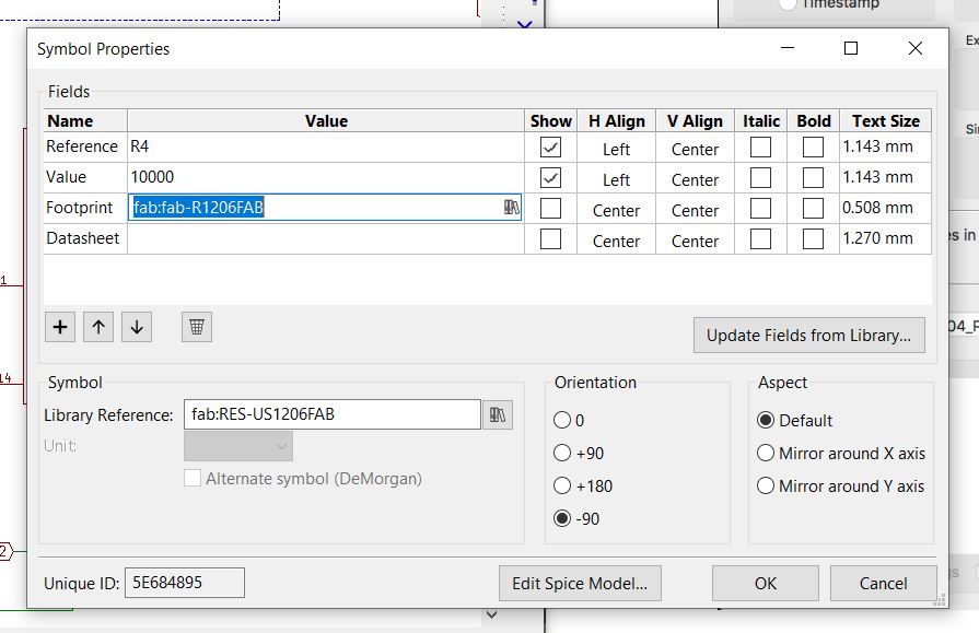
Now that we have all the components needed, along with the additional button and LED, we need to check whether the footprints are correctly linked. Hover over a component and click on "e", as we did earlier, and check the bar that says footprints. In my case, all my component's footprints were not connected and I had to go in each one of them to find the footprint. You can do that by clicking on the little button in the footprint bar and searching for it.
Generate Netlist
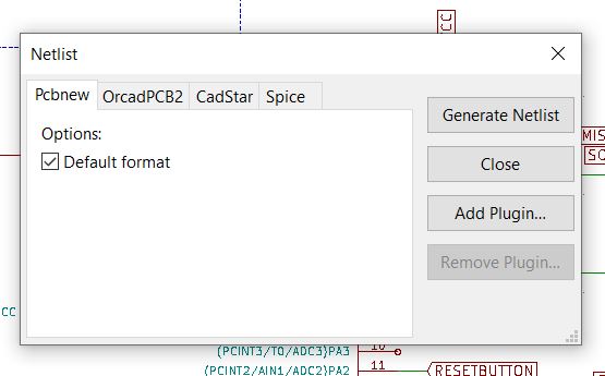
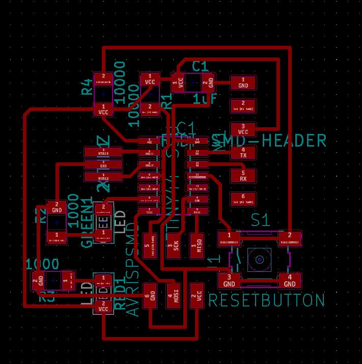
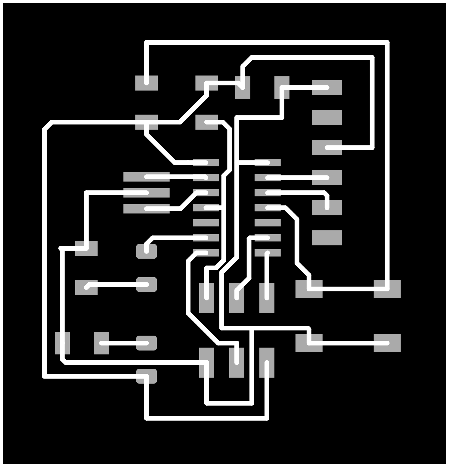
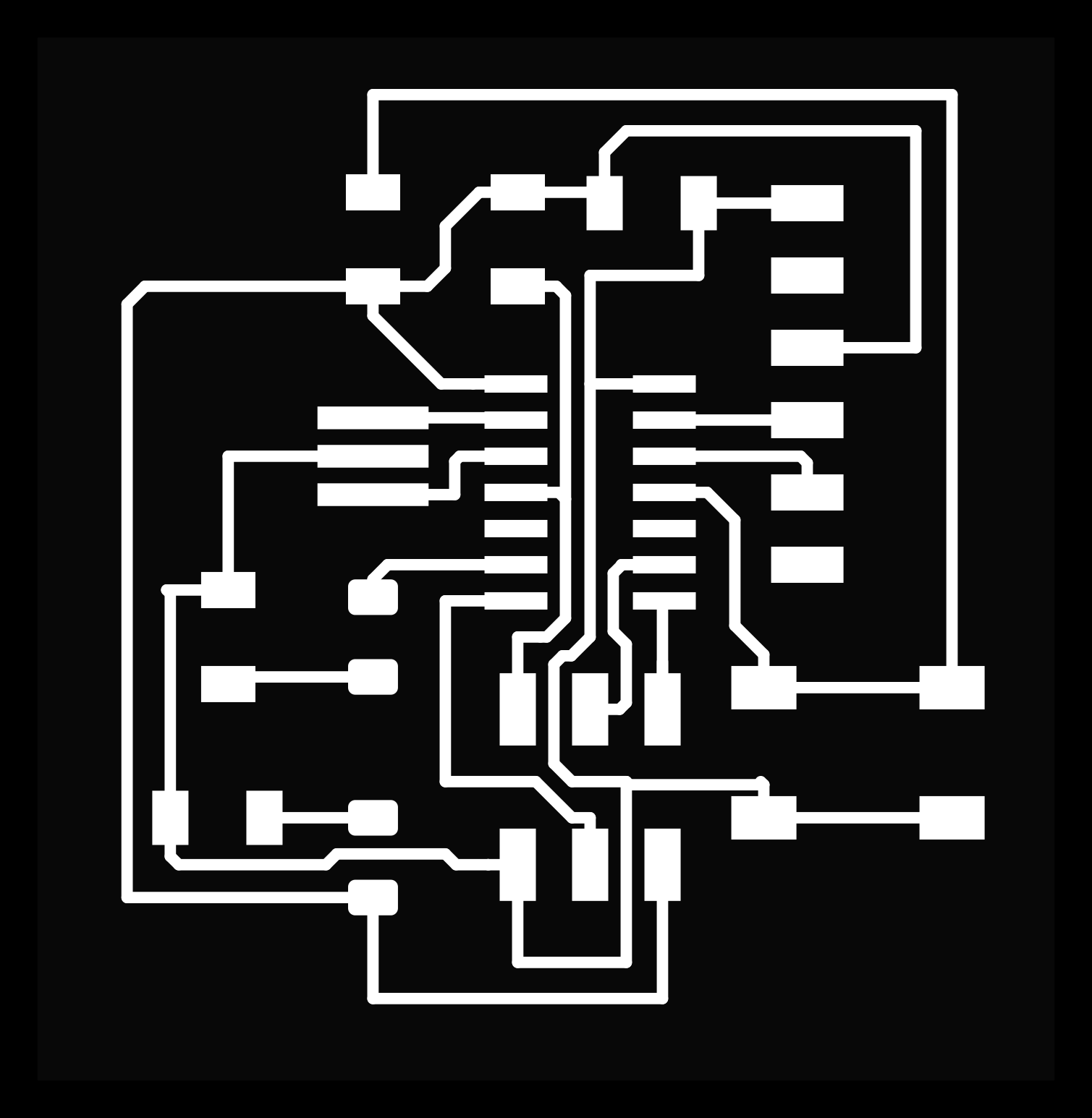
Once all the footprints are linked you will need to "generate netlist" found on the top 4th from the right horizontal symbol. It will ask you to select the file location for the netlist and then you can close the eschema window. The next step is to open the PCB Layout Editor, 3rd horizontal symbol from the left. Once you open the editor you select your netlist and you will find a bunch of components placed in an odd manner in the window. The task now is to find the most suitable way to place the components. The white lines are confusing and tangled but they are there to guide how the connections are and they update themselves when you move the component. I began untagling the components on my own to test if I could find a good placement and also make it aesthetically pleasing. However, after a lot of frustration with it, I decided to take a look at the board image from the Fabacademy folder and use it as the guideline.
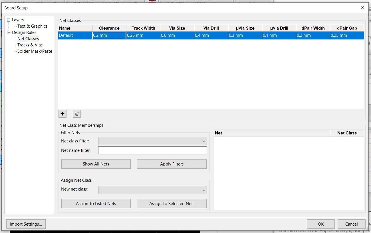
Specify Design Rules
Access the design rules by clicking on file > board setup > design rules. There you will need to fix the settings to make sure that there is always enough spaces between the traces and also the components. The settings that I used were as follows.
Draw Traces
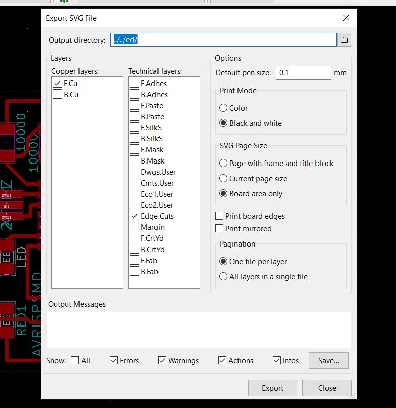
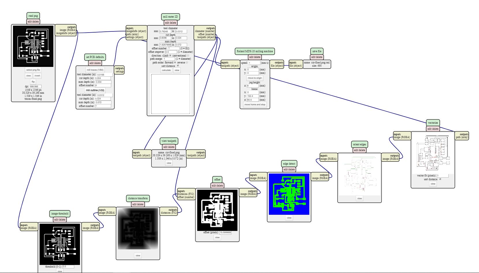
Now that our design rules are set and the components are places in an "optimum" position we can begin drawing the traces. I drew and redrew the traces around 4-5 times as every time I was drawing I would accidentally have some connections too close to them and when I would try to use mods there turns out to be connections when they are not needed. To fix the issue I needed to decrease the grid size 0.0508mm as the traces snap to the grid. Once I decreased the gride size, I had more control over the movements of the traces and was able to keep good distances between each other and the components. Once the drawing is where you want it to be, you can export the traces in SVG. I chose to export each layer at a time because it would make it easier to use for the next steps.
Prepare the file in Inkscape
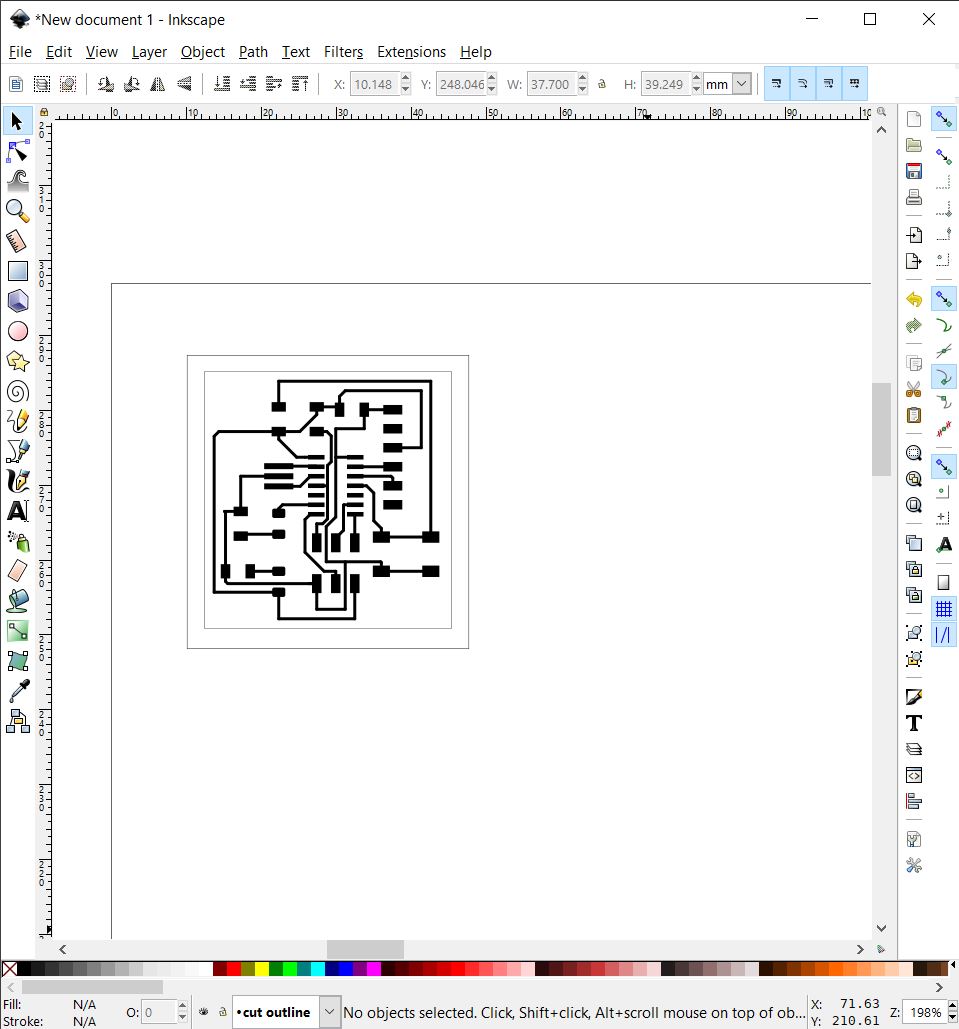
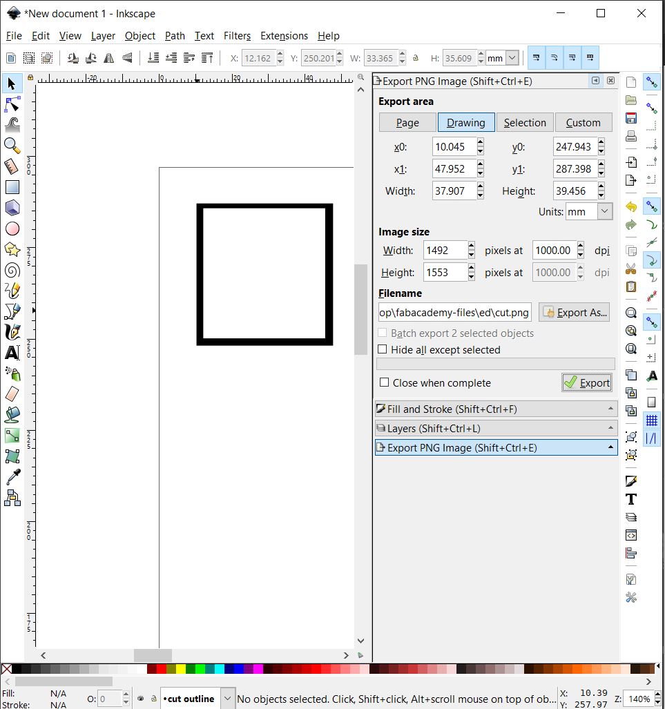
The next step is to prepare the exported files for milling. Open the svg files in inkscape, if you downloaded them in different layers then you will need to import all the different files. Once they are imported assign one layer for the traces and another for the outline cut. As the traces and the outline use different drill bits for the milling. When the SVG drawing is in inkscape, it will come with the traces in black and the negative space in white. You will need to invert the colors to make the background in black and the traces in white. That way it will be ready to mill. Once done inverting, export them into png. Make sure to export wih the drawing selected and the image size points at 1000 dpi.
Prepare for machining
Now that our board is prepared we will set it up in mods. Open mods and the steps are: - make sure that the correct milling machine is selected. If not, right-click > programs > open server programs > then select the machine. I am using the Roland mill MDX-20 PCB png.
- Once that was selected, I changed the speed of the machine to 3 mm/s,
- checked that the origin is placed at xy 0,
- and changed the z jog height to 6 mm/s.
- The next step is to select the correct drill bit in the "set PCB defaults" window, for traces use the 1/64 and for outline cuts use the 1/32.
- Add the save file module by right-click > modules > open server modules > file save.
- Once the previous steps are done, go to the mill raster 2D window and calculate.
- Once calculated, it either opens a new window with the claculated traces or it directly asks you to save the .rml file.
You can check, preliminarily, whether the board will be successful or not by making sure you have distances between unconnected components and traces.
Machining
Milling
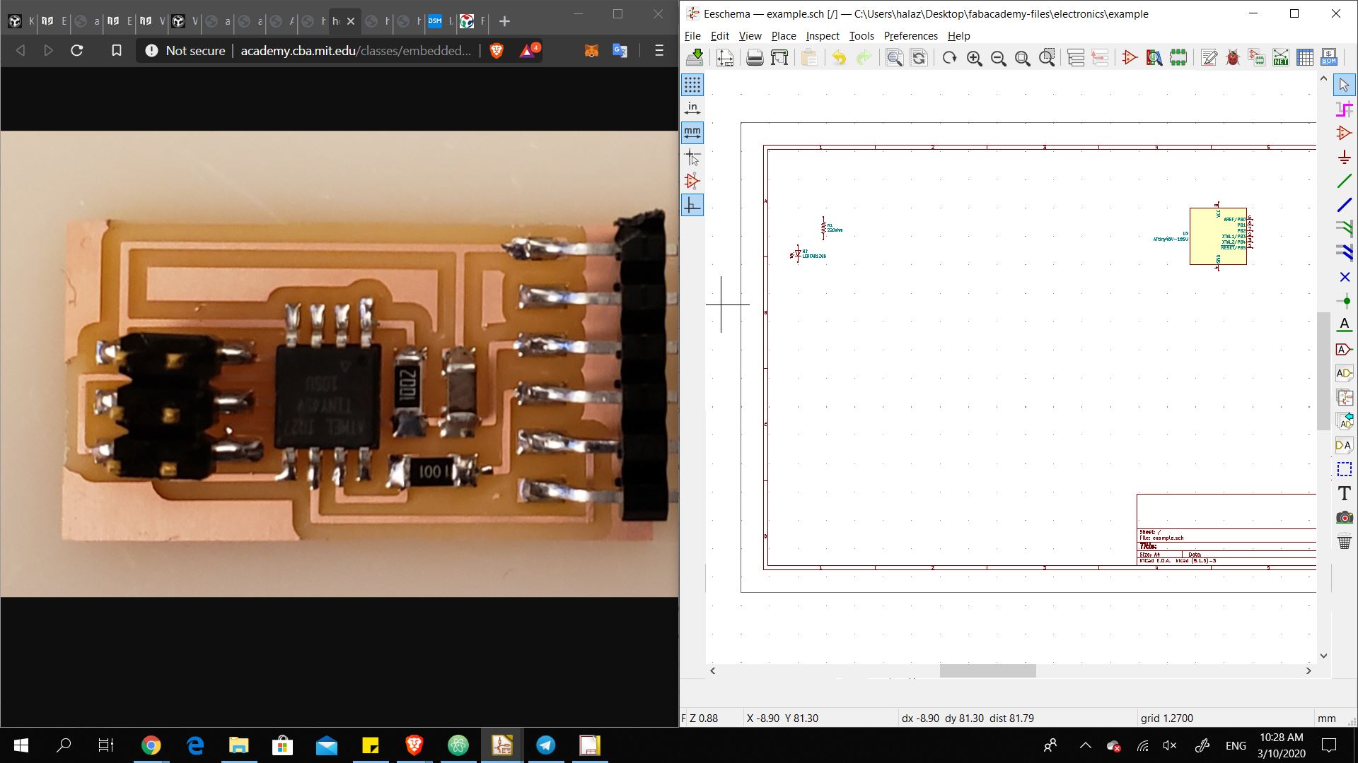
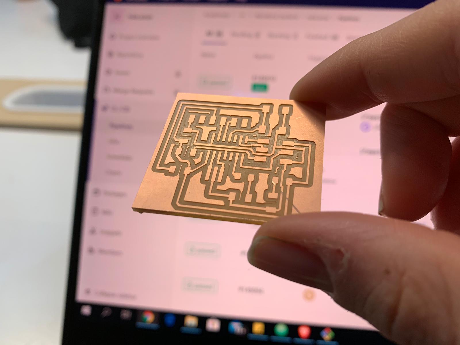
As I used the Roland MDX-20 to mill my board and the software connected to this machine is designed by a tutor in the FabLab, Eduardo Chamorro Martin. The interface is made really simple, all the buttons are labeled in a way where anyone with no experience could still use the machine successfully. I stuck the PCB to the bed at the home corner, front left, and began by setting the x and y to that corner. Once the xy are set I move to setting the z-0. In the first try, I set the z wrong by doing it through the software and when I loaded the file to mill, it did it in the air. Thankfuly, the error happened in the air and the machine did not plunge into the PCB, which would have cost me the 1/64 drill bit!
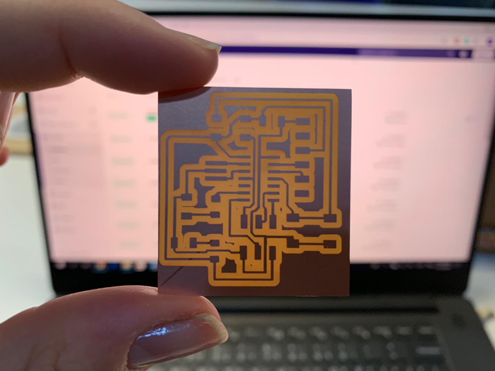
I set up the z-0 again and reuploaded the file and began the cutting. The traces came out clean and the distances between them were sufficient, although I can not be sure until I check with the multimeter. Once the traces are done, I needed to change the bit to the 1/32 and upload the outline cut files. Once the cut files were done, the PCB board was ready to be tested with the multimeter.
Soldering
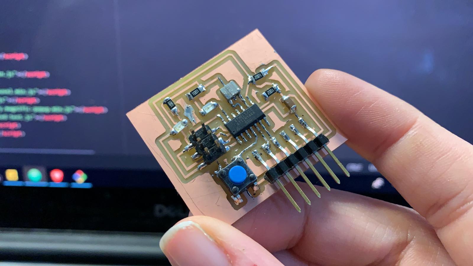
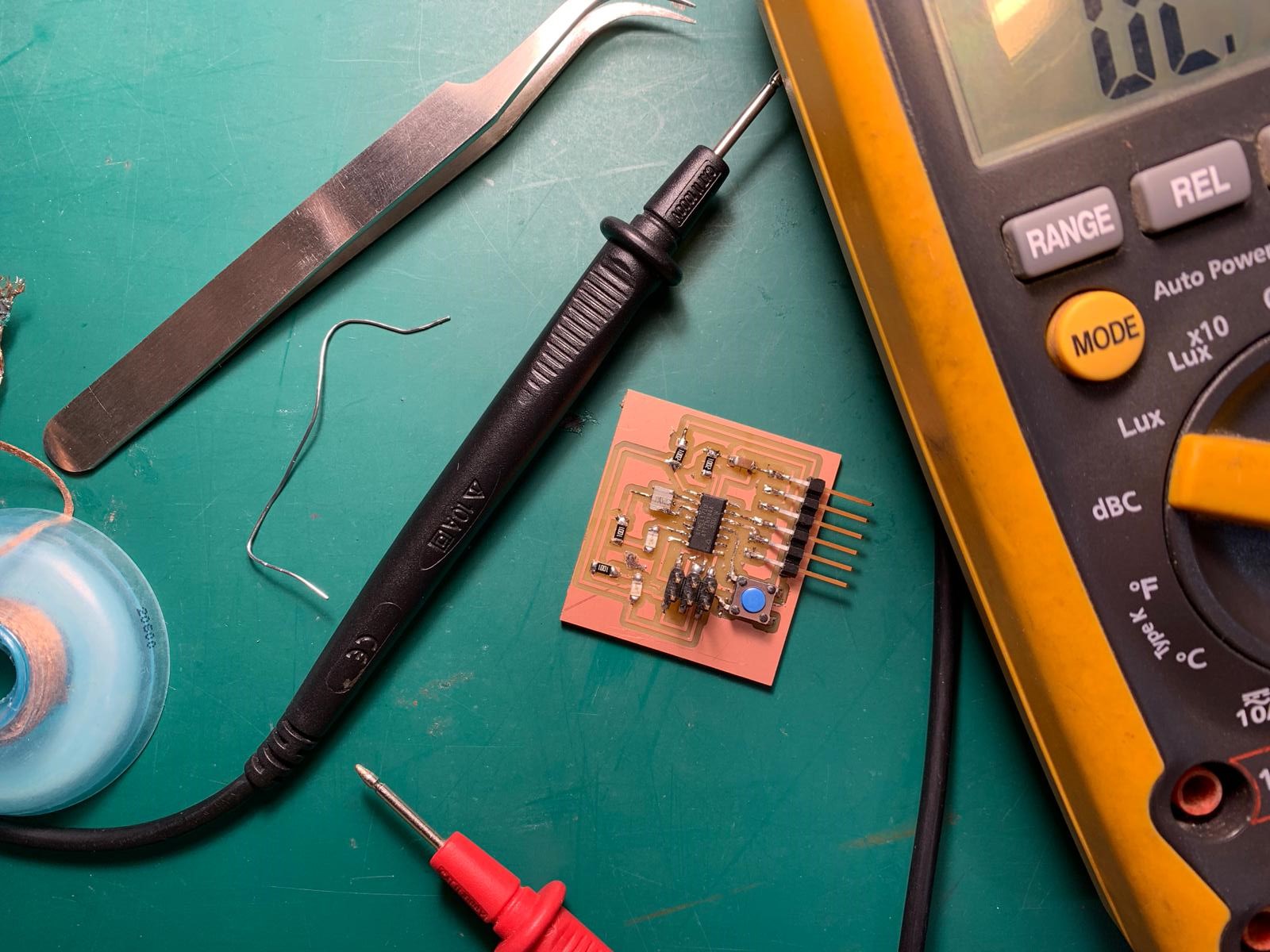
Once the milling was done, I collected the components needed and began to solder them. As this is the second time we have soldered components, it felt much easier this time around. Instead of taking over an hour for the ISP ATtiny 45 (which I did last time) it only took half an hour for the ATtiny 44. It was also much clearer to find the soldering mistakes, when the points are not shiny or when they are leaving a pointy mark.
Group/Individual Assignment
Checking with the Multimeter
For this assignment, we were not able to do the group project together and so we individually checked the direction of each one of our boards.
To make sure that the directional components were correctly placed and that the connections were clean, I used the multimeter. The multimeter will allow us to see if there is continuity or if there were shorts. Place the knob at the wifi looking option and check the board design to check the continuity of your connections and design. If there are any connections where there shouldn't be you can use the copper tape to remove the solder. If the continuity is obstructed then double check to make sure if the directional components are correctly placed and if they are then check if the component legs are touching the board.
Final Thoughts
To me, the most important part of this week's assignment is understanding the workflow needed to design and produce the boards which is why I tried to outline them as neatly and in correct order to follow them in the future. I have also improved much in soldering!
Files