Sketch
Project Description
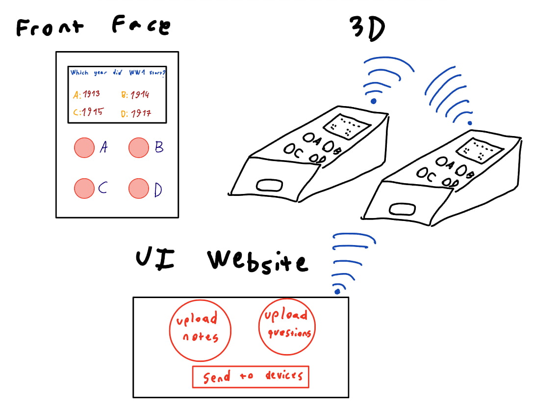
My Fab Academy final project is an interactive learning device designed to support quiz-based studying and in-class competitions.
The system is inspired by digital quiz platforms and focuses on physical interaction combined with networked content delivery. The questions are prepared on web either uploaded by the user or generated by a custom AI model. The device displays questions, multiple-choice answers, and basic competition feedback such as timing and scores.
Device Overview
The device consists of:
- An OLED display used to show questions, answer options, and simple status or score information
- Four physical push buttons, mapped to multiple-choice answers (A, B, C, D)
- A microcontroller with Wi-Fi capability to receive quiz data and send user responses
User interaction is intentionally simple: the learner reads the question on the screen and selects an answer using the physical buttons.
Scope and Fab Academy Relevance
This project is suitable for Fab Academy as it allows me to:
- Design and fabricate a custom enclosure
- Design and produce custom PCBs
- Program embedded systems
- Implement input and output devices
- Explore networking and communication between devices
Project Timeline
| Task / Weeks | 1 | 2 | 3 | 4 | 5 | 6 | 7 | 8 | 9 | 10 | 11 | 12 | 13 | 14 | 15 | 16 | 17 | 18 |
|---|---|---|---|---|---|---|---|---|---|---|---|---|---|---|---|---|---|---|
| Preparation and Research | X | |||||||||||||||||
| System Concept & Sketching | X | |||||||||||||||||
| CAD – Early Enclosure & Layout | X | X | ||||||||||||||||
| Prototyping – Interface (Display & Buttons) | X | X | ||||||||||||||||
| Prototyping – Electronics (Schematic) | X | |||||||||||||||||
| Implementation – PCB Design | X | X | X | |||||||||||||||
| Implementation – Embedded Programming | X | X | X | |||||||||||||||
| Implementation – Networking | X | X | ||||||||||||||||
| CAD – Enclosure Refinement | X | X | X | |||||||||||||||
| Production & Assembly | X | X | X | |||||||||||||||
| System Integration & Testing | X | X | ||||||||||||||||
| Optimization & Refinement | X | X | ||||||||||||||||
| Documentation | X | X | ||||||||||||||||
| Finalization & Project Completion | X | |||||||||||||||||
| Presentation Prep & Evaluation | X | X |
CAD Design
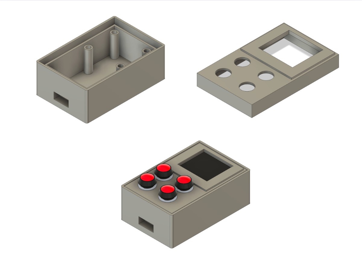
In Week 2, I developed the parametric 3D design of my final project enclosure using Fusion 360. I translated initial layout ideas into constrained sketches, extruded and shelled the main body, and iteratively refined the geometry to accommodate real electronic components. By importing reference models, adjusting clearances, and adding tolerances for 3D printing, I validated fit and manufacturability through multiple revisions. This process established a solid, editable CAD foundation that will support future iterations, assembly decisions, and fabrication steps of the final project.
3D Printed Model
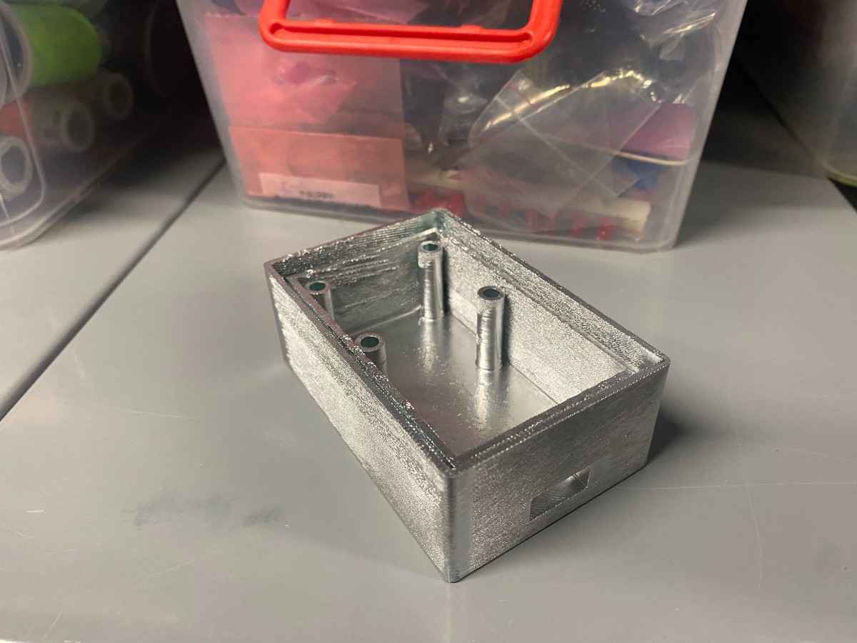
I printed my designs as I exported them as STL files from Fusion360. I printed my designs on Bambulab P1S printers using PLA filament. My buttons fit perfectly on the top part.
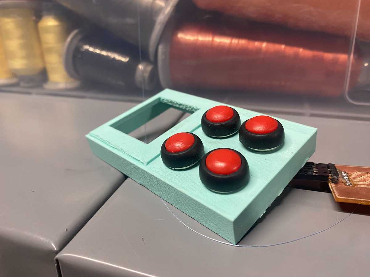
Below is the body printed, I spray painted it silver to give a nice aesthetic.
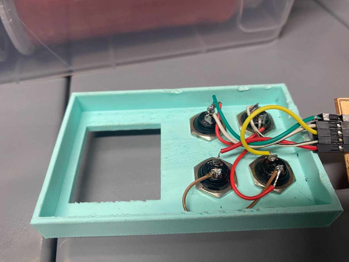
I then soldered the GND’s of the buttons together and also soldered jumper cables on the buttons to connect them to my PCB.
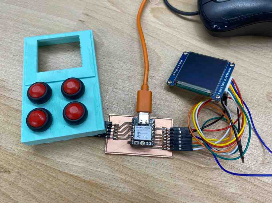
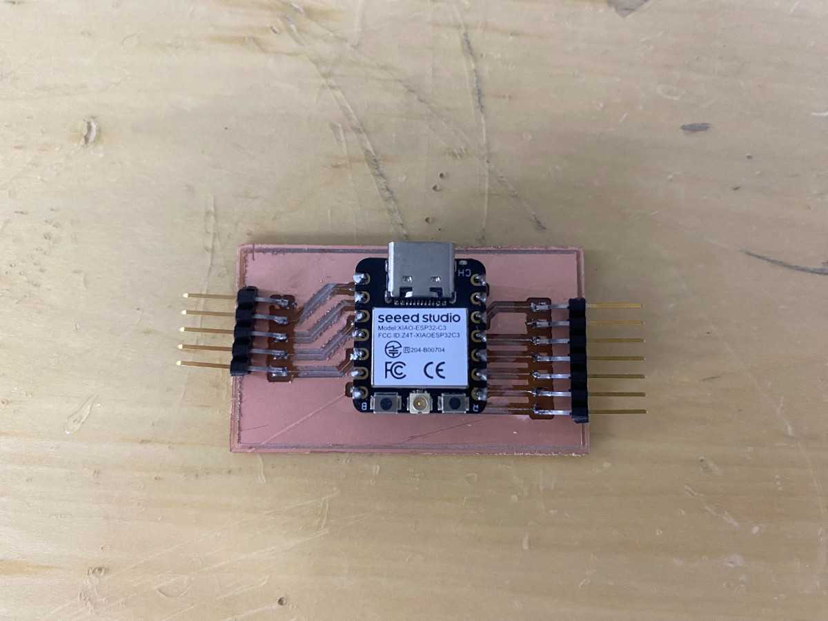
PCB Design and Production
You can find the details of my design and production of my PCB in my weekly documentation. I fabricated the PCN on the SRM-20 machine and soldered my components on.
![]()
Here’s the PCB with the ESP microcontroller.
Below is the fully connected wiring of my final project components.