Learning Objectives
- Select and use software for circuit board design
- Demonstrate schematic → PCB workflows
- Produce multiple custom PCBs for different purposes
Hero Shot
1. Introduction
This week, I designed two completely separate PCBs, each for a different purpose:
Board A — Servo Driver PCB (Learning Board)
A small board made specifically to learn the full electronics workflow:
- Creating symbols
- Selecting footprints
- Correcting ERC/DRC
- Fixing connector orientation
- Adding a level shifter
- Preparing files for milling
This board is not part of my final project.
Its purpose was entirely educational: to practice designing PCBs confidently before building the real final project hardware.
Board B — Final Project PCB (OLED + Buttons Interface)
A second PCB designed for my actual final project, containing:
- A 7-pin SSD1351 OLED connector
- Four push buttons
- Custom PH2.0-7 footprint
- 3.3 V–only domain
- Clean extended routing and layout
These two boards are separate because they serve different roles in my Fab Academy journey:
| Board | Purpose | Voltage Domain | Why Separate? |
|---|---|---|---|
| Servo PCB | Practice electronics → learn PCB workflow | 3.3 V + 5 V, level shifting | Required TXB0104 + servo current handling |
| Final Project PCB | Real hardware for final project | Pure 3.3 V | Screen + buttons, custom connectors |
Creating the learning board first allowed me to make mistakes safely, fix them, and gain confidence before designing the actual final project hardware.
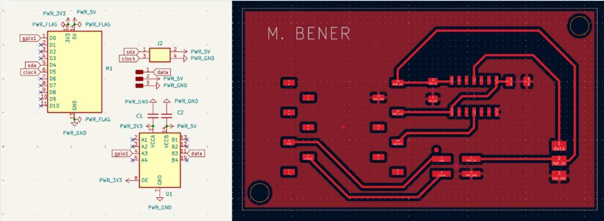
2. Board A — Servo Driver PCB (Learning Board)
2.1 Schematic Design Workflow
I started with the Module_XIAO_Generic_SocketSMD symbol to represent the ESP32-C3 Super Mini.
Mistake v1 — Adding the Servo Directly to PCB
The servo motor should not exist on the PCB. It must be connected externally.
Mistake v2 — Using Three 1×1 Headers
These are mechanically unstable and don’t match lab inventory.
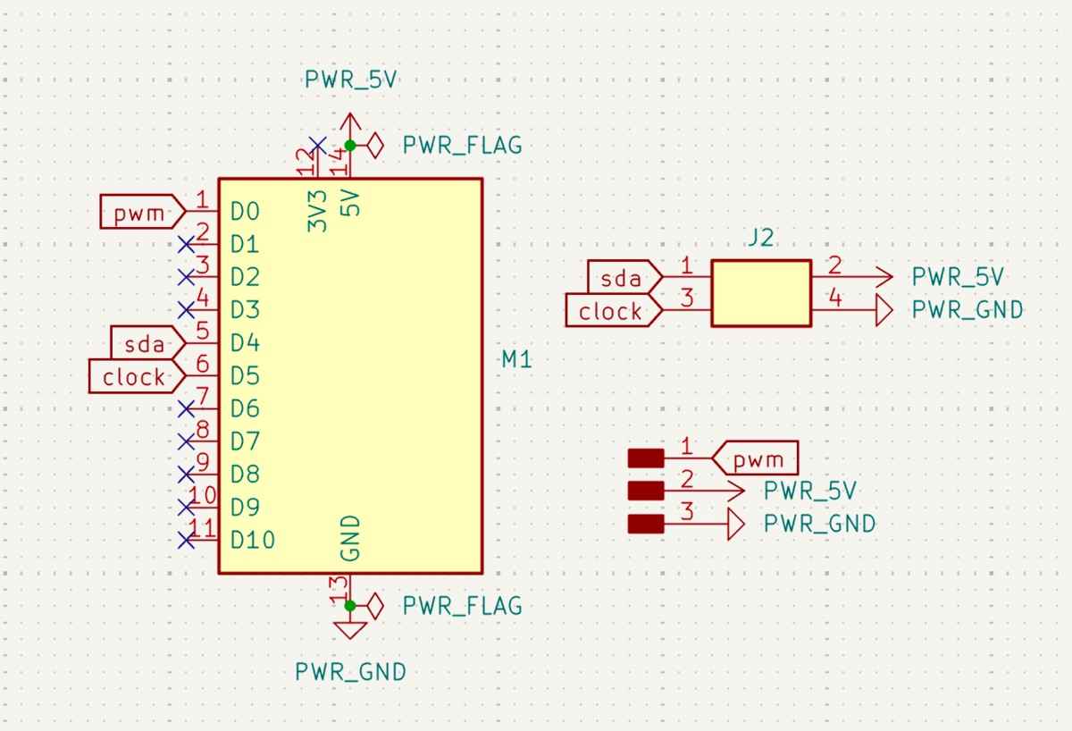
Corrected Schematic (v3)
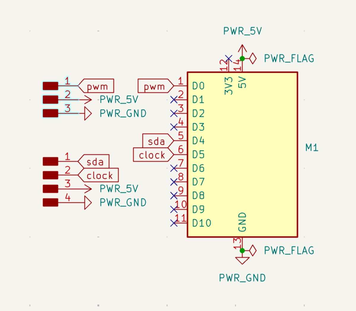
✔ Proper 3×1 and 4×1 headers
✔ ESP32-C3 symbol correctly used
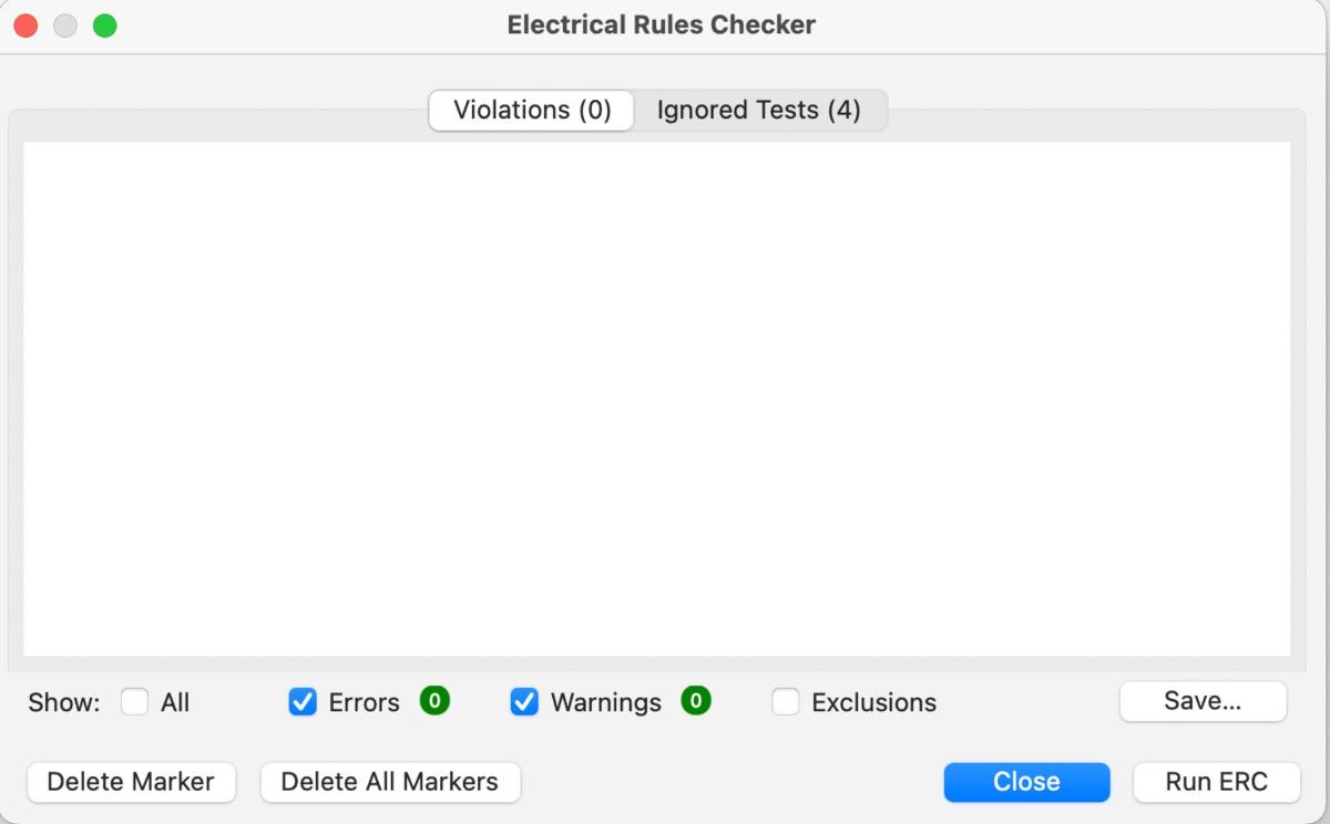
✔ ERC = 0 errors
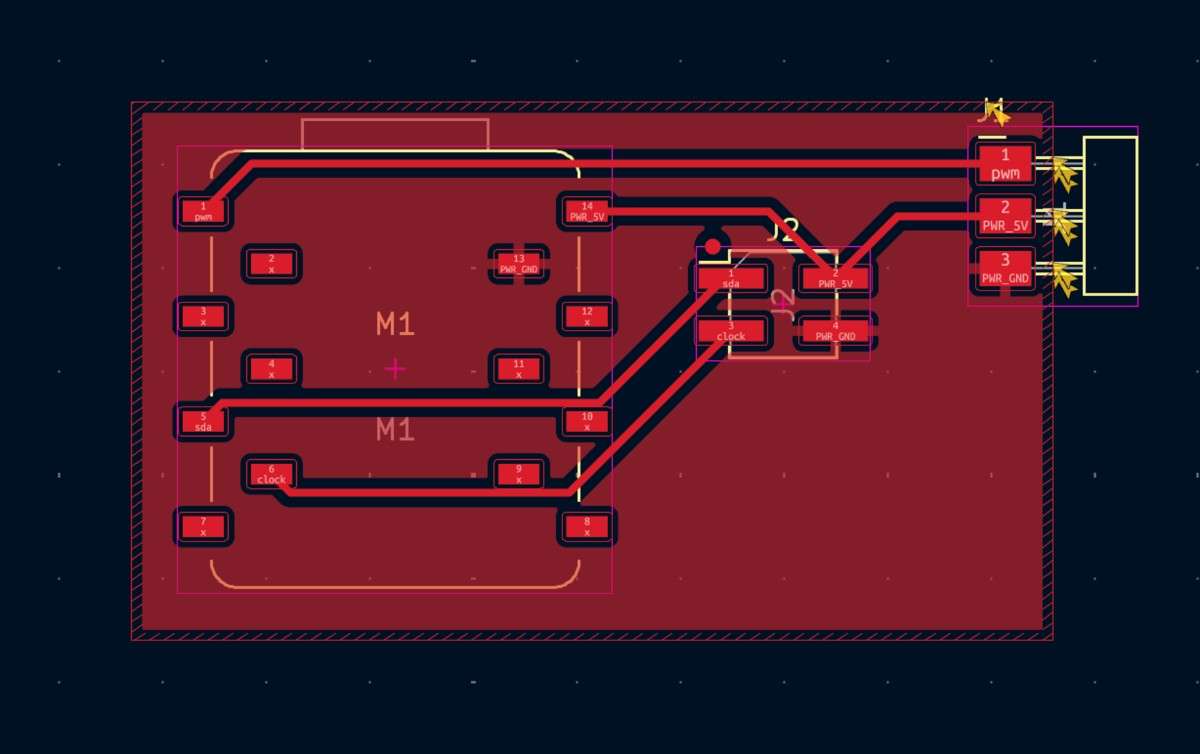
2.2 PCB Layout
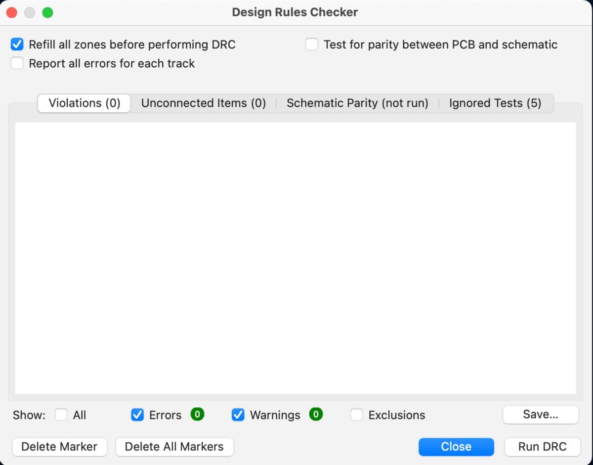
PCB v3 (First Working Version)
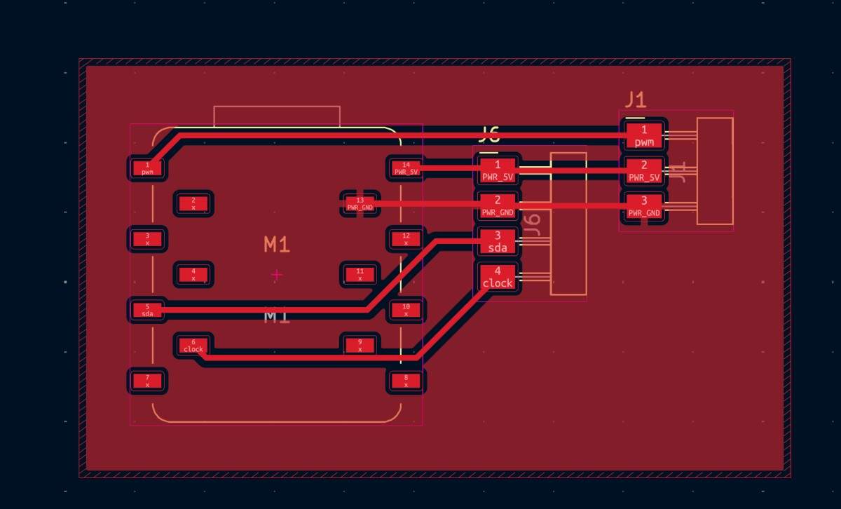
DRC = 0 Errors
2.3 Mentor Feedback & Improvements
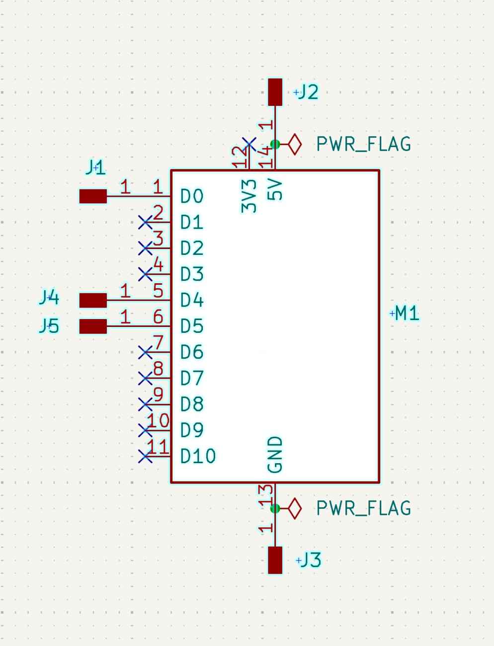
1) Header Orientation
I accidentally used horizontal headers, but the lab only stocks vertical headers.
I replaced footprints → aligned them to PCB edge for mechanical strength.
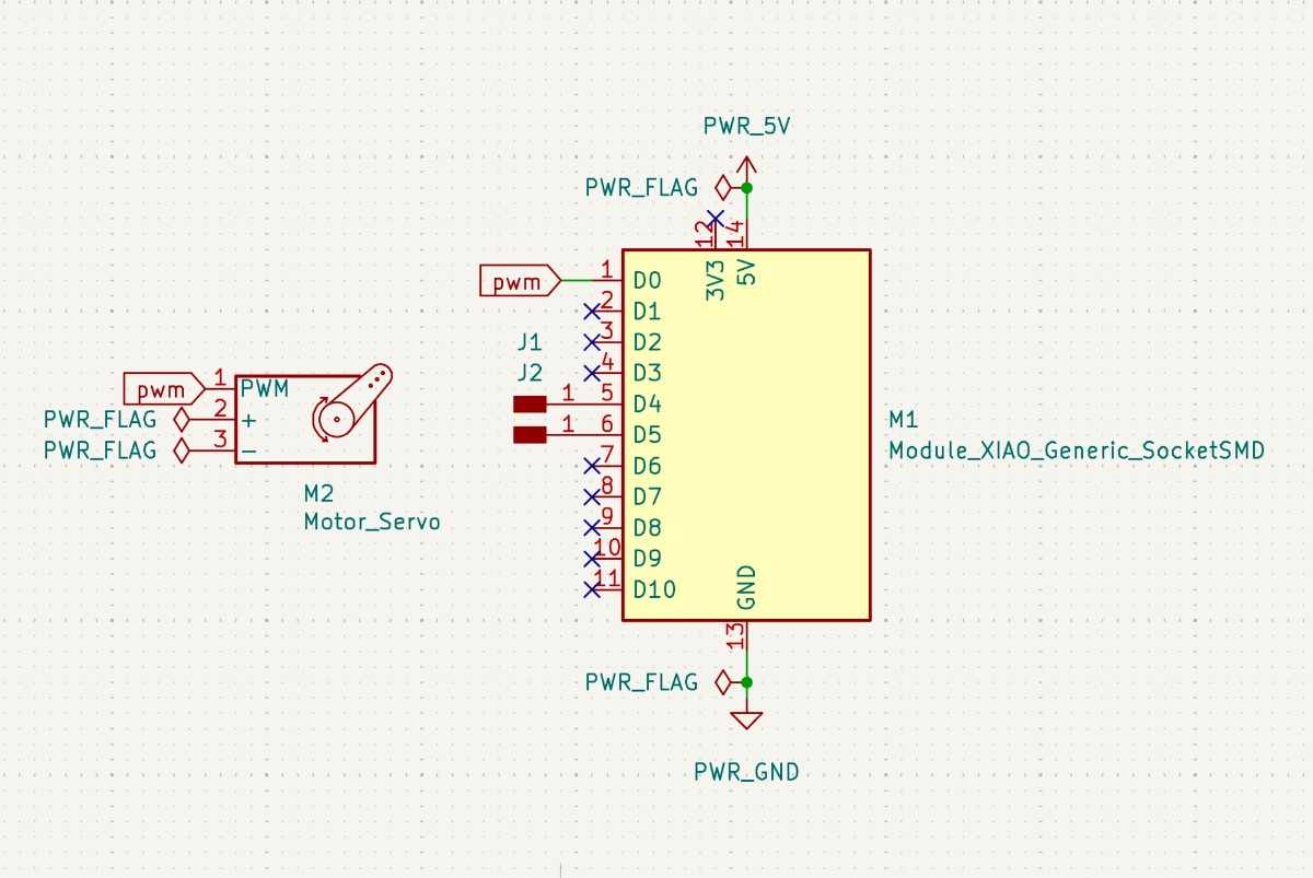
2) Adding TXB0104 Level Shifter
Servo expects 5 V logic, ESP32-C3 outputs 3.3 V → risky PWM behavior.
Added:
- TXB0104 bidirectional level shifter
- 0.1 µF decoupling capacitors
- 10 µF bulk capacitor on 5 V rail
Updated Schematic & PCB
2.4 Final Servo Board After Fixes
Mechanical Fix
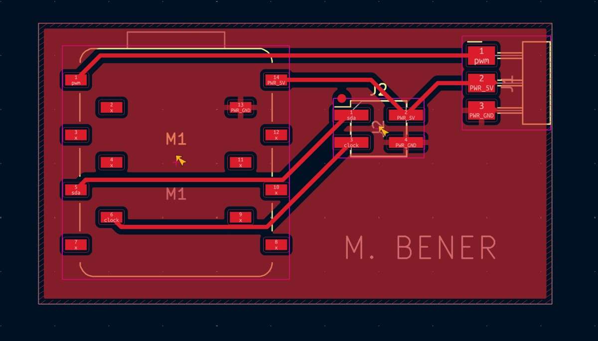
Final Schematic
Final Routed PCB
Mounting Holes Added
2.5 Bill of Materials (BOM)
| Component | Qty | Purpose |
|---|---|---|
| ESP32-C3 Super Mini | 1 | Microcontroller (3.3 V logic) |
| TXB0104 level shifter | 1 | Shifts PWM 3.3 V → 5 V |
| 3×1 vertical pin header | 1 | Servo connection |
| 4×1 vertical pin header | 1 | GPIO breakout |
| 2×2 vertical header | 1 | I²C |
| 1×7 female header | 2 | ESP32-C3 sockets |
| 0.1 µF ceramic cap | 2 | TXB0104 decoupling |
| 10 µF cap | 1 | 5 V bulk filtering |
| M3 mounting holes | 4 | Mechanical |
| FR-1 PCB | 1 | Milled board |
2.6 Power Analysis
Servo is the dominant load
- Requires 5 V
- High current (stall current can exceed 600 mA)
- Must not draw power from ESP32’s regulator
Final Power Routing
- 5 V rail → Servo V+
- 3.3 V → ESP32-C3 + TXB0104 VCCA
- 5 V → TXB0104 VCCB
- Ground common everywhere
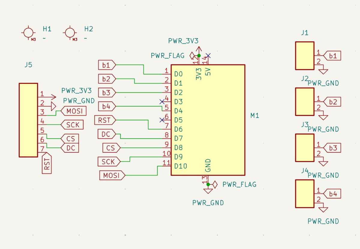
3. Board B — Final Project PCB (OLED + Buttons)
This PCB is not a practice board.
It is the real PCB for my final project.
Circuit Simulation
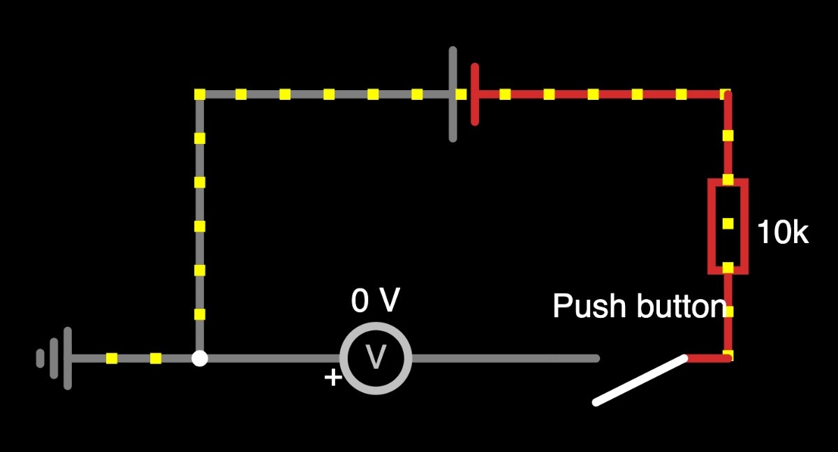
To verify the behavior of the button input circuit used on my PCB, I simulated the circuit using a two-terminal 3.3 V DC power source and a push button.
The simulation represents the electrical logic of the button input and allows observation of voltage changes at the probe point when the button is pressed or released.
Simulated Circuit Configuration
The simulated circuit consists of:
- A 3.3 V DC source (positive and negative terminals)
- A push button (SPST)
- A probe point representing the GPIO input
- A common ground reference
In this configuration, the input node is connected to ground when the button is open, and connected to 3.3 V when the button is pressed.
Button Open (Not Pressed)
When the button is open, the input node is not connected to the 3.3 V source and is instead held at ground potential.
- Measured voltage at probe point: ~0 V
- Interpreted logic level: LOW
This represents the idle state of the button in the simulated circuit.
Button Closed (Pressed)
When the button is pressed, the circuit closes and directly connects the input node to the 3.3 V supply.
- Measured voltage at probe point: ~3.3 V
- Interpreted logic level: HIGH
This shows a clear and stable logic transition when the button is actuated.
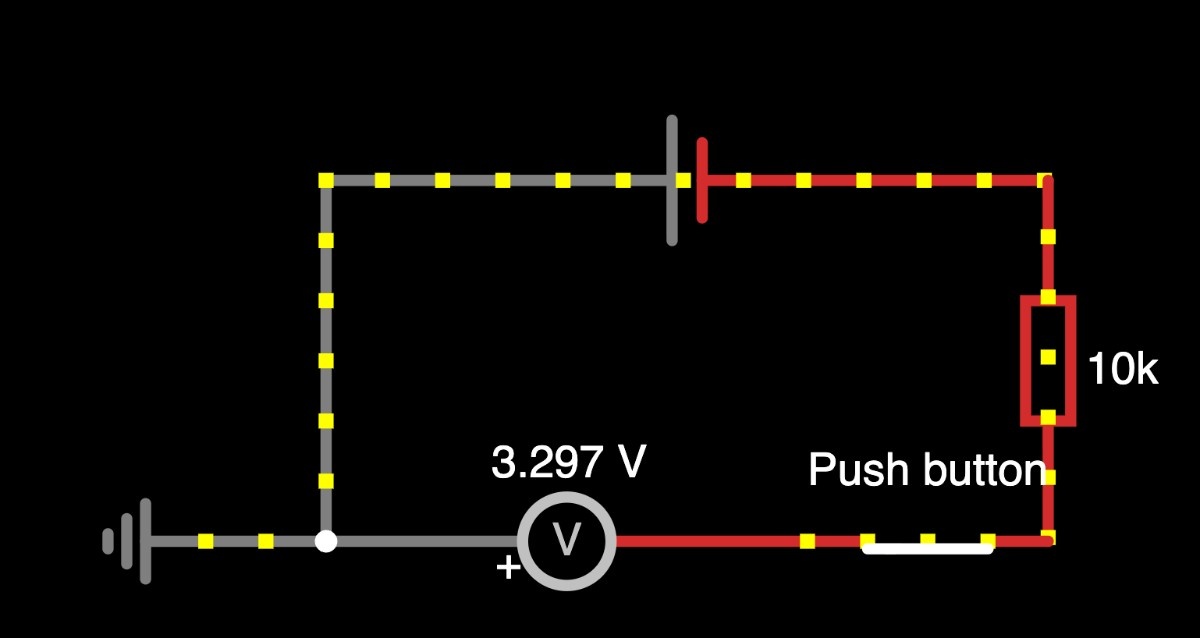
Simulation Outcome
This simulation confirms that:
- The input node changes predictably between 0 V and 3.3 V
- The button produces clean digital logic levels
- The circuit behavior is electrically valid and safe for microcontroller GPIO inputs
The simulation was used to understand and verify signal behavior and complements physical testing performed later on the actual PCB. This simulation was used to verify and reason about digital input behavior and voltage levels, while final electrical behavior was confirmed through physical testing on the fabricated PCB.
3.1 Wiring Plan
OLED Screen (SSD1351, 4-Wire SPI)
| OLED Pin | ESP32-C3 Pin | Description |
|---|---|---|
| VCC | 3V3 | Power |
| GND | GND | Ground |
| SCK | D9 | SPI Clock |
| MOSI | D10 | SPI Data |
| RST | D6 | Reset |
| DC | D8 | Data/Command |
| CS | D7 | Chip Select |
All pins operate at 3.3 V, so no level shifting is required.
Push Buttons
| Button | ESP32-C3 Pin | Details |
|---|---|---|
| BTN1 | D0 | Internal pull-up |
| BTN2 | D1 | Internal pull-up |
| BTN3 | D2 | Internal pull-up |
| BTN4 | D4 | Internal pull-up |
Each button connects between GPIO → GND.
Connector Choice (Button Side)
- Button terminals: 2.8 mm female spade
- PCB side: Chosen → JST-PH 2-pin
- Compact
- Reliable
- Easy to replace buttons
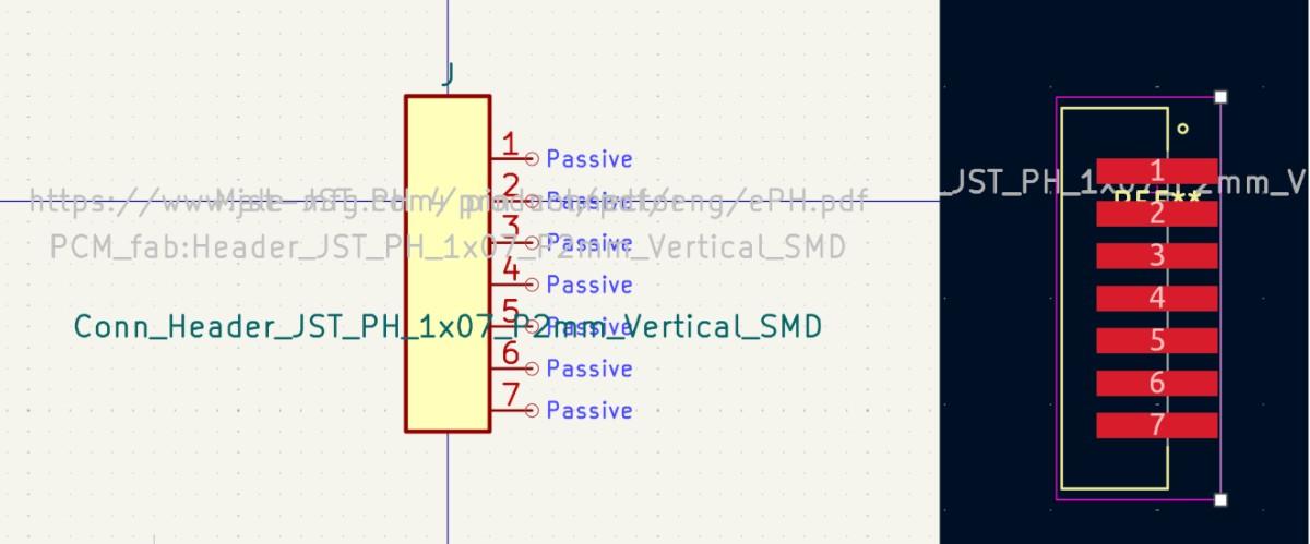
3.2 PH2.0 7-Pin OLED Connector Problem
The fablibrary has:
- PH2.0-3 pin
- PH2.0-4 pin
But not PH2.0-7 pin.
They cannot be combined because the mechanical side pads collide.
3.3 Solution — Designing a Custom Symbol and Footprint
Steps
- Open Footprint Editor
- Duplicate PH2.0-4C footprint into custom global library
- Delete side mechanical pads
- Duplicate pad 4 → move down by 2.00 mm
- Create pads 1–7 with perfect grid alignment
- Rebuild silkscreen
- Redraw courtyard
- Save footprint
- Created matching 7-pin symbol in Symbol Editor and assigned the footprint.
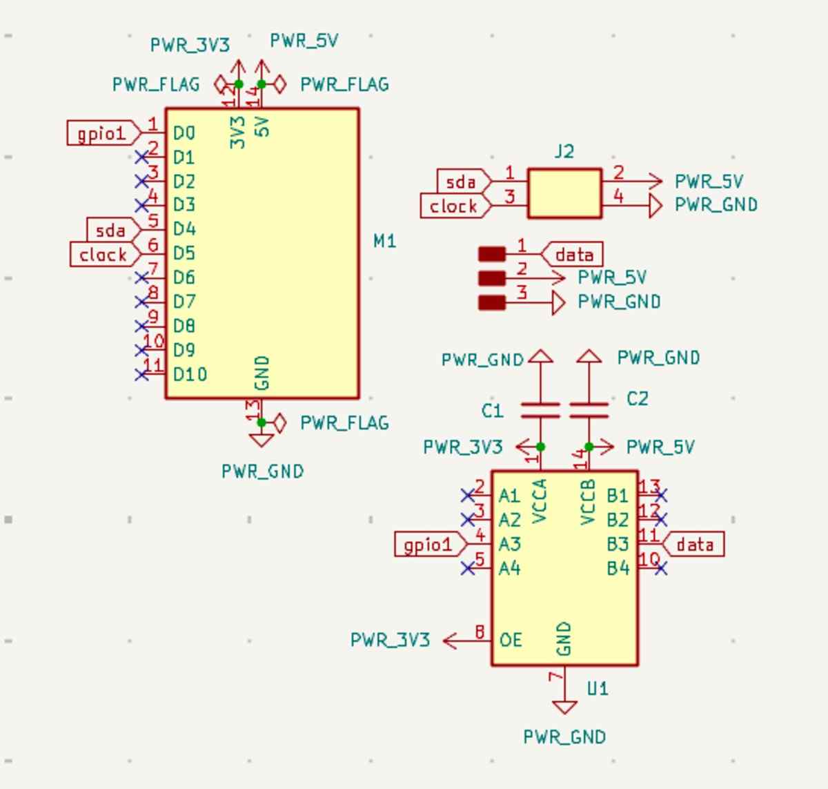
3.5 Updated Schematic (Final Project PCB)
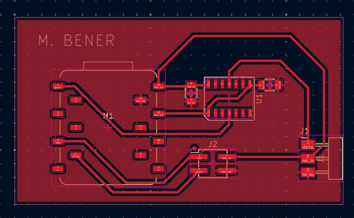
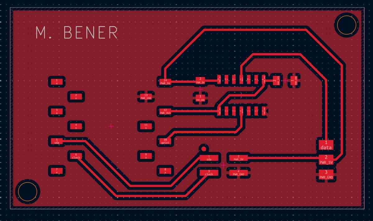
3.6 PCB Layout
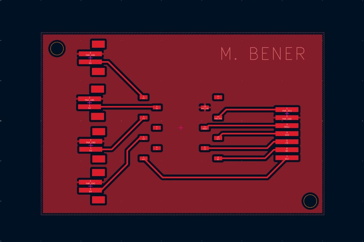
✔ Clean routing
✔ Correct clearances
✔ Correct connector spacing
✔ All 3.3 V domain
✔ Perfect for final project enclosure
4. What I Learned
Electronics Design
- Separated design goals: learning board vs. final project board
- Selecting correct footprints and headers
- Creating custom footprints and symbols
- Using level shifters properly
- Designing connectors with mechanical stability
PCB Workflow
- Snapping to grids (2.54 mm + 2.00 mm)
- Designing for solderability
- Verifying all designs using ERC + DRC
- Understanding lab inventory constraints
System-Level Thinking
- Why boards should NOT be combined
- Voltage domain separation (3.3 V vs. 5 V)
- Designing small, modular PCBs
5. Group Project
You can check our group project here