Learning Objectives
- Described the process of tool-path generation, milling, stuffing, de-bugging and programming
- Demonstrate correct workflows and identify areas for improvement if required
Hero Shot
1. Introduction
This week focused on electronics production: milling the PCB, soldering all components, debugging, and finally actuating a servo motor using the board I designed in Week 6.
Starting from the RML files generated in Week 6, I produced my custom PCB using the SRM-20 milling machine, then soldered all components, learned from several failed attempts, and eventually built a fully working microcontroller development board.
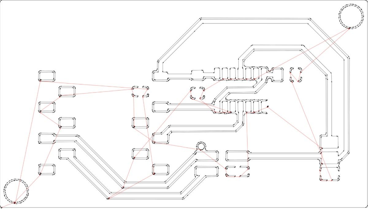
2. Generating Toolpaths
To mill the PCB, I needed to export my KiCad design properly and prepare the layers in Inkscape before generating toolpaths in Mods.
Exporting Layers
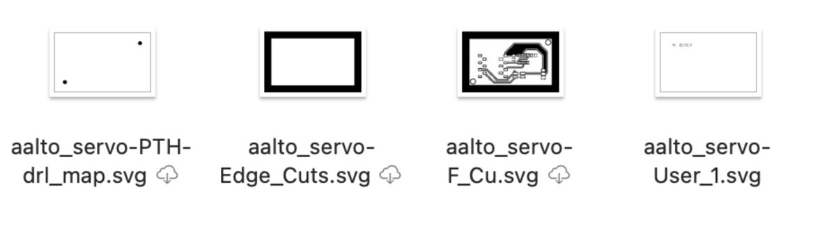
I exported four separate PDFs:
- Copper layer
- Edges layer
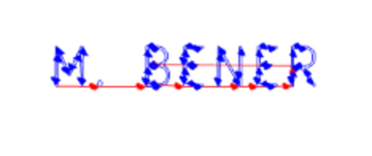
- User1 layer (for name engraving)
- Drill layer (mounting holes)
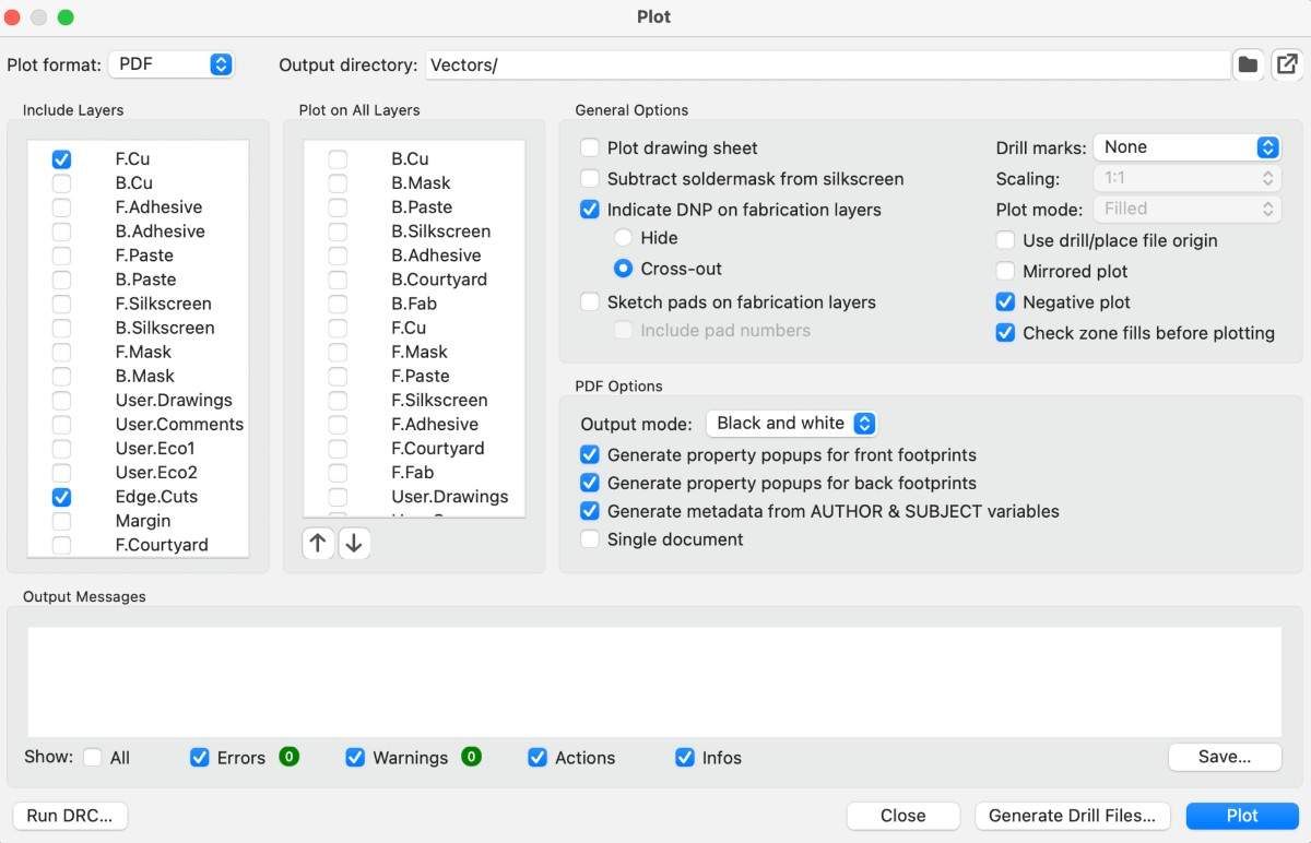
In the Plot window, I enabled Negative Plot.
We avoid exporting SVG directly from KiCad because the KiCad SVG output is unreliable and breaks scaling.
Preparing SVGs
I imported each PDF into Inkscape and prepared them:
- Resized all layers to identical canvas size
- Changed colors
- Engraving + copper layers remain black (milled regions)
- Drill map and text changed to white on black for proper detection
- Exported each finalized layer as SVG
Exported SVG Files
Turning to Toolpaths
I used modsproject.org → Programs → Open Program → Roland SRM-20 → Mill 2D PCB.
The UI is shown below:
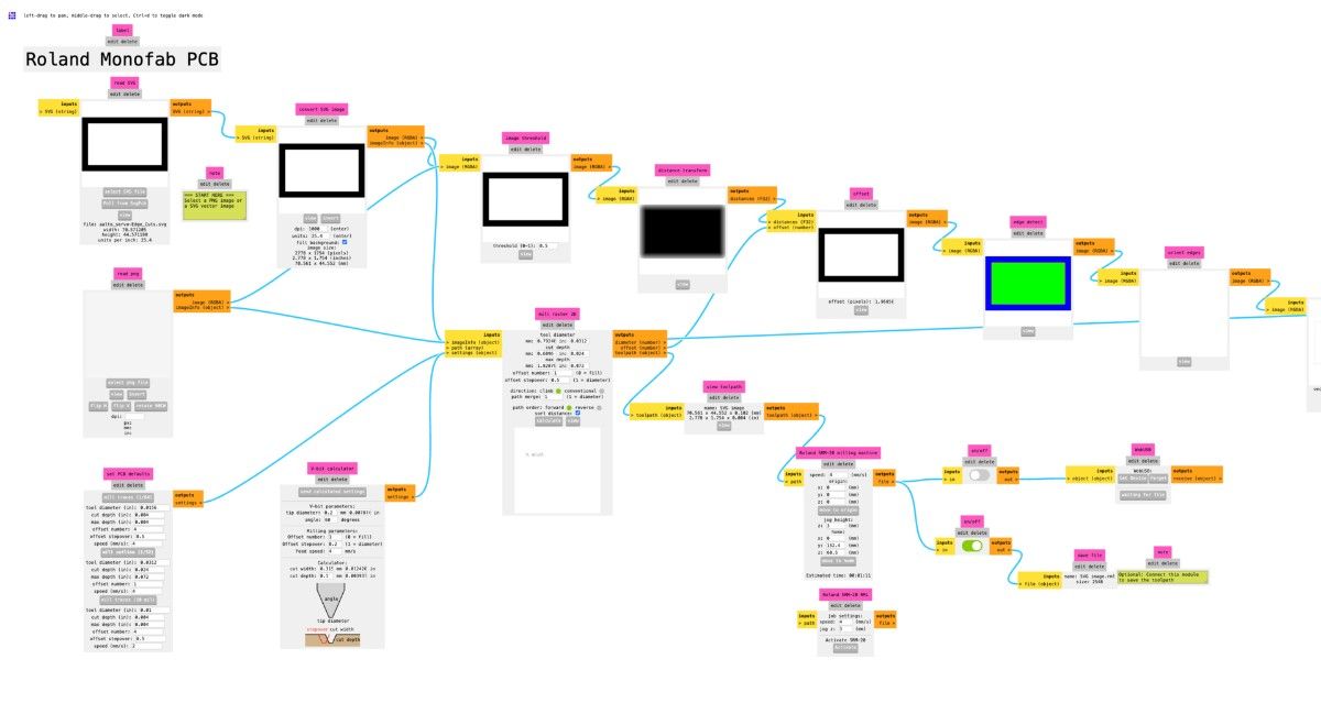
After loading each SVG, I set the appropriate mill settings.
Example Output – Copper Layer
Example Output – Name Engraving Layer
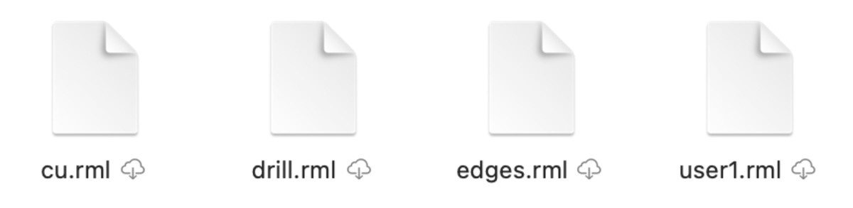
Output Files
Errors & How I Solved Them
Issue 1 — Milling Air (Z too high)
Mods has a default origin of (10,10,10).
My first job milled completely in the air.
Fix: Set origin to (0,0,0).Issue 2 — Wrong Offsets
Mods default offset for copper engraving was 4, meaning it would mill the outline four times.
Fix:- Copper layer (engraving): offset = 1
- Name engraving: offset = 4
- Outline cutting: offset = 1
After correcting these settings, the RML files worked perfectly for milling.
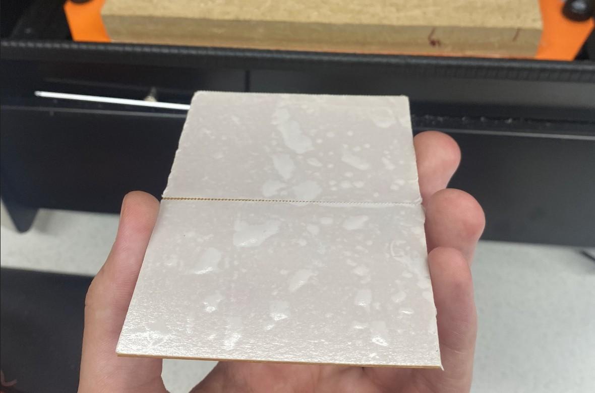
3. PCB Milling
The first step was preparing the copper clad for milling. I covered the back of the copper board with double-sided tape to ensure firm adhesion inside the milling machine.
Preparing the Copper Clad
After taping, I mounted the copper clad inside the Roland SRM-20:
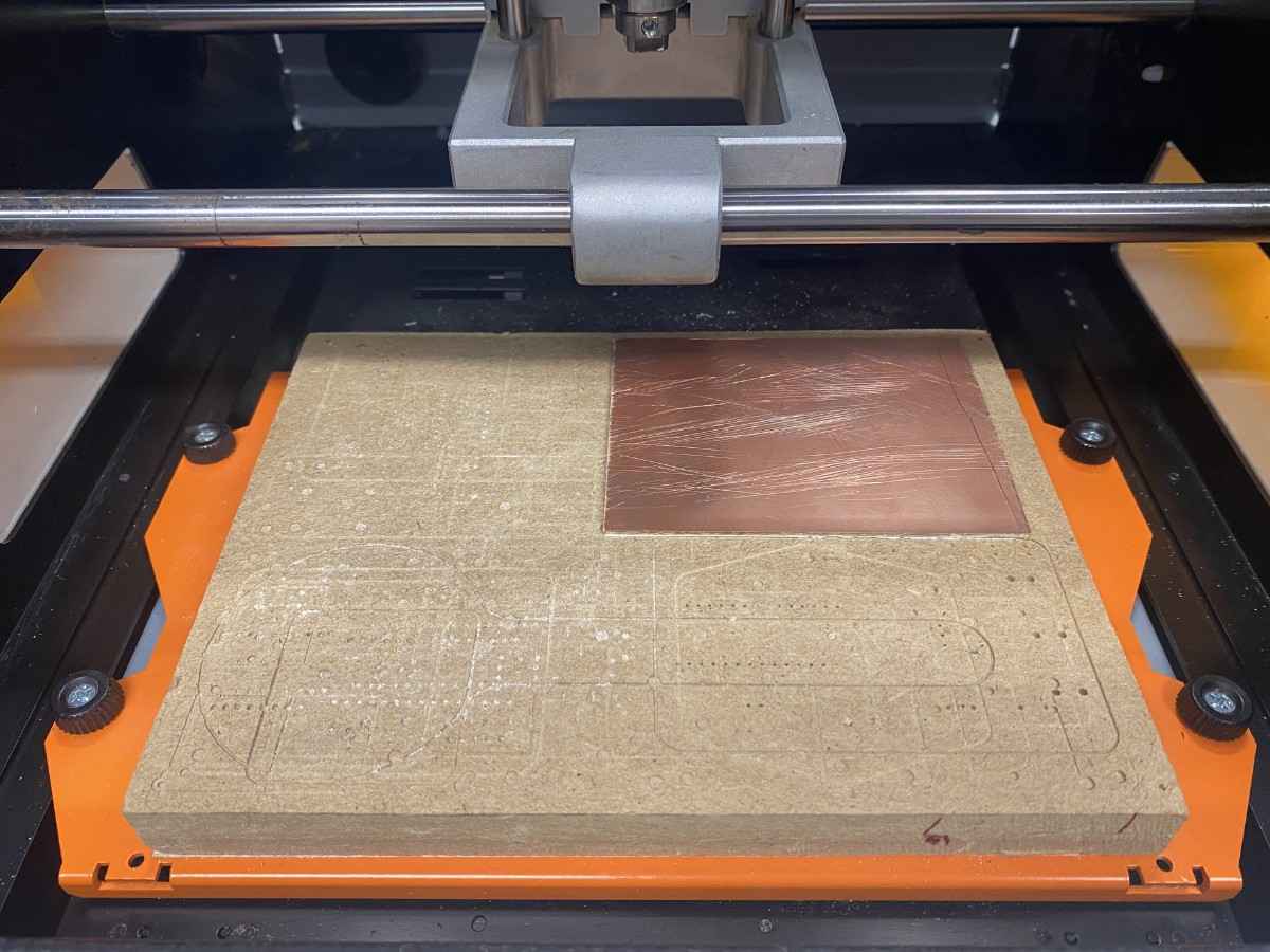
Setting Up the Machine
Inside the machine, I:
- Set the XY origin
- Lifted Z by ~3 mm
- Inserted the 0.8 mm end mill (not too tight—tightening too much can break the bit)
- Loaded drill.rml and edges.rml for this 0.8 mm tool
After finishing all 0.8 mm jobs, I swapped in the 0.2 mm end mill and ran:
- cu.rml (copper milling)
- user1.rml (name engraving)
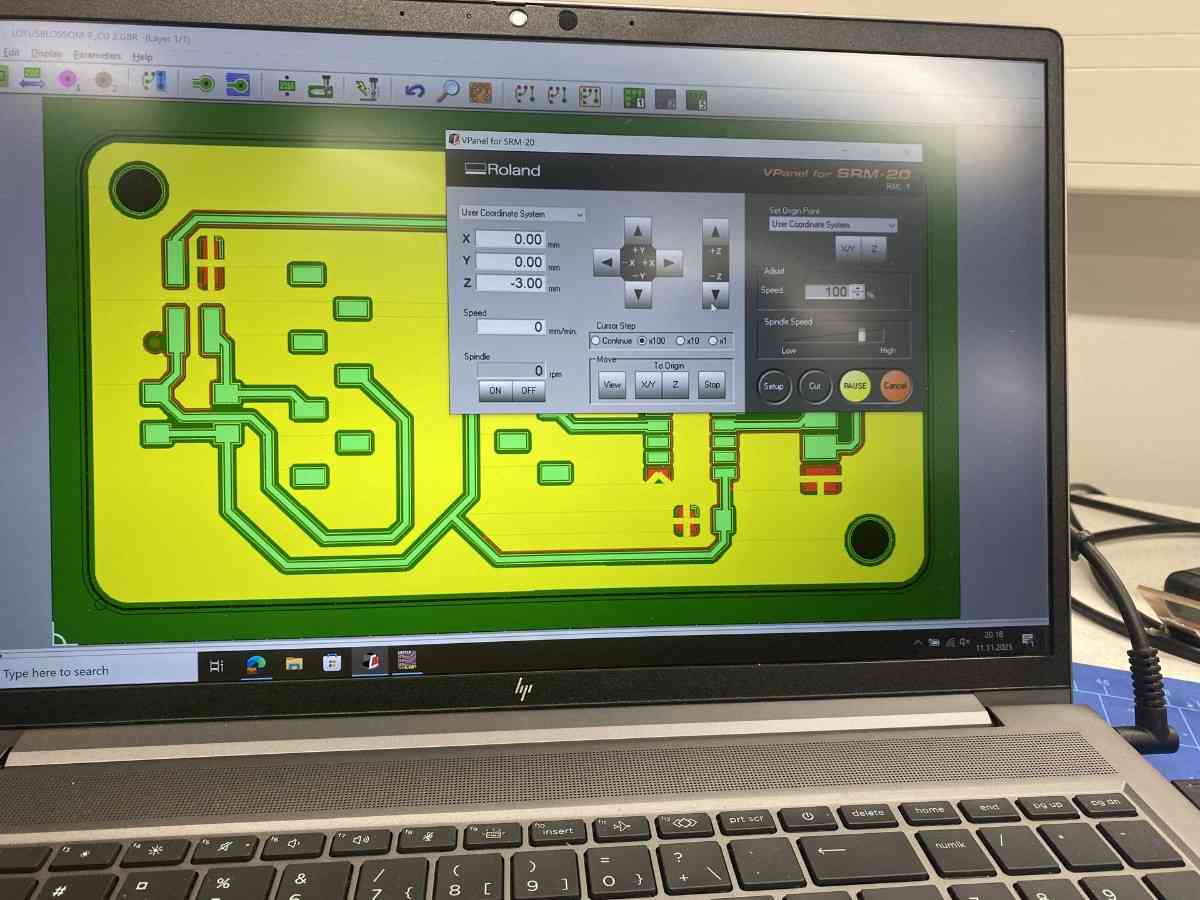
Below is the control computer running VPanel (NOT CopperCAM):
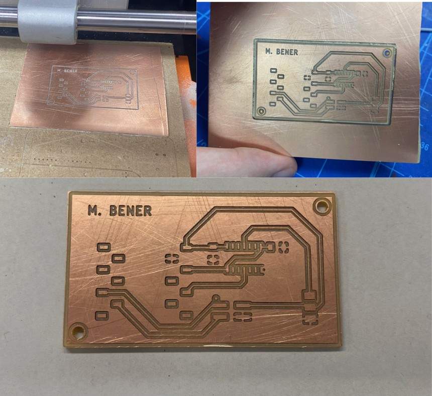
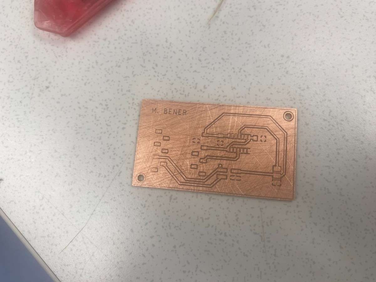
Milled Board Results
Electrical Testing
After milling, I verified all traces with a multimeter (continuity mode).
The multimeter beeps only when two points are electrically connected, which helps identify broken traces or shorts.
My board passed all continuity tests.
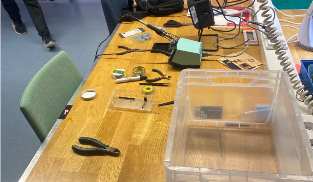
4. Soldering & Assembly
The next step was soldering all components onto the milled PCB.
Component Layout
Before soldering, I arranged all components on the board to visualize placement:
First Soldering Attempts
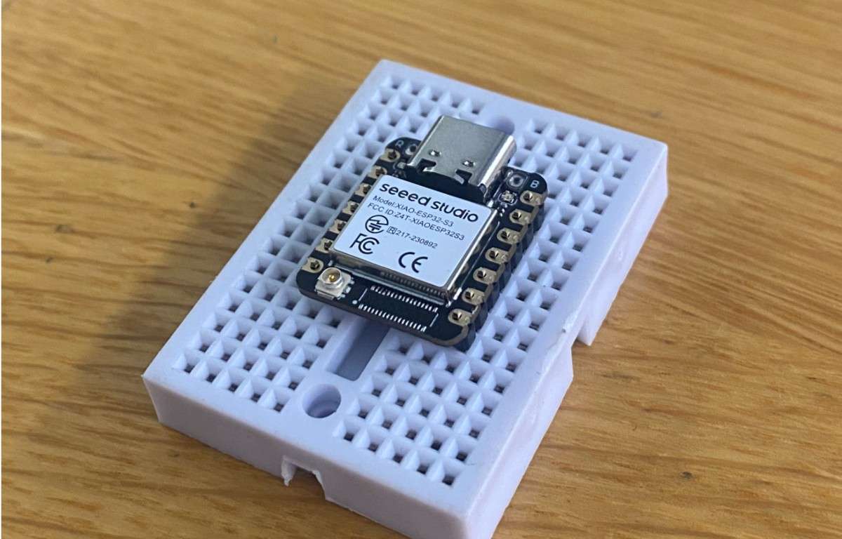
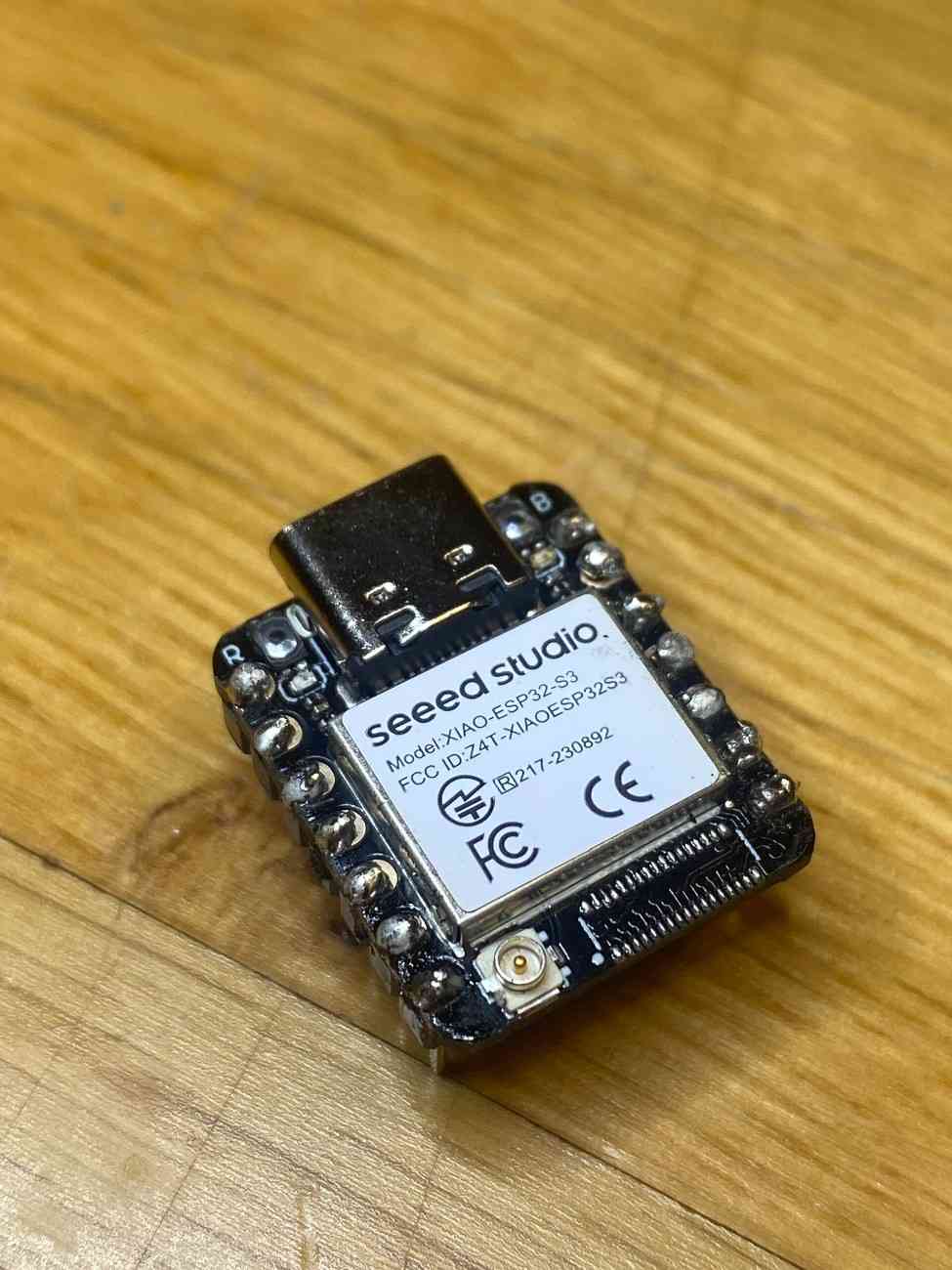
I started by soldering header pins onto the ESP32 module directly (not onto the PCB yet):
Soldering Setup
Before Soldering
After Soldering
Then I soldered:
- A 3×1 horizontal socket for servo output
- A 2×2 header for I²C
These came out clean, but later I encountered several board-ending mistakes.
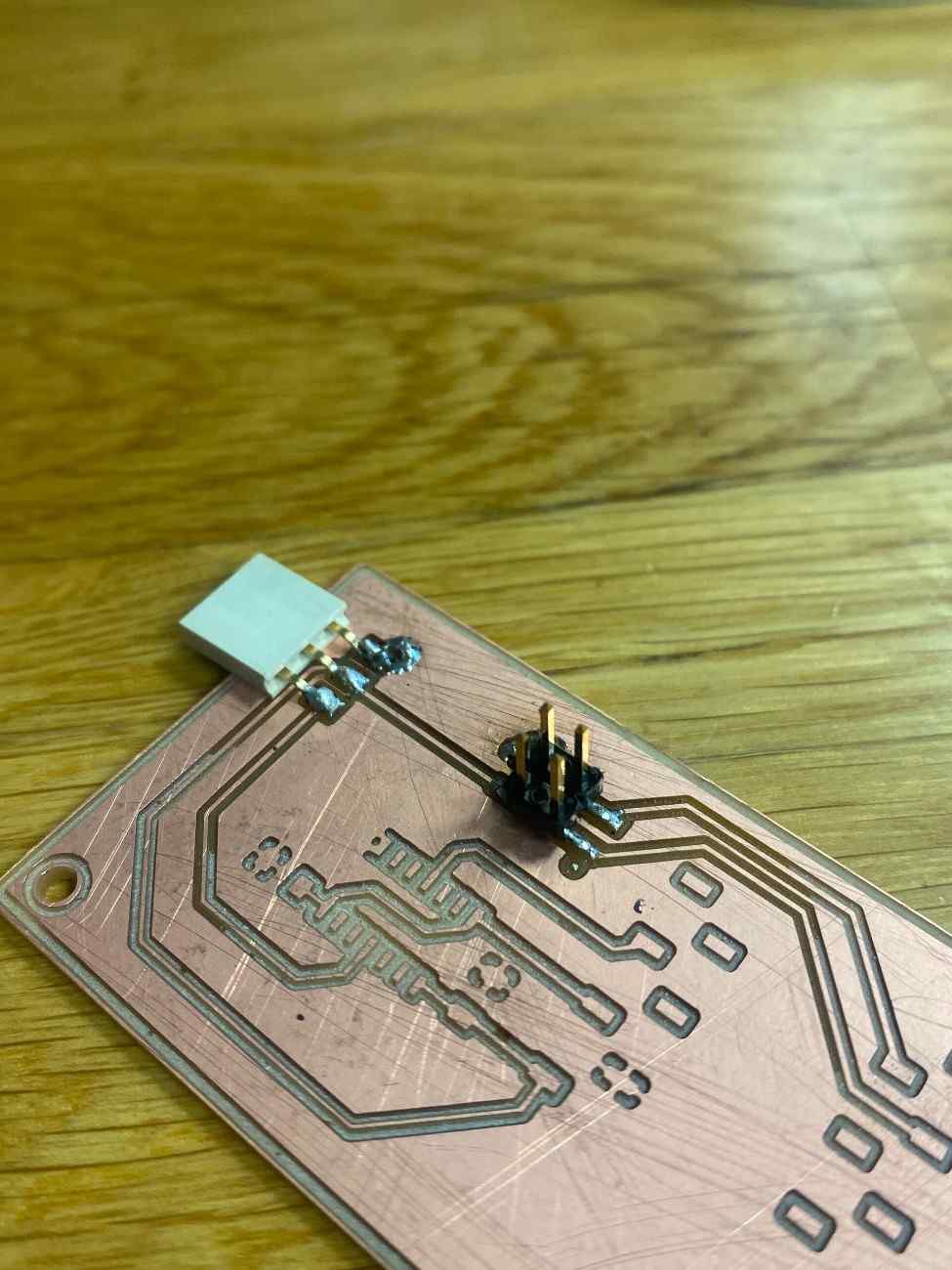
Failed Boards
Fail #1 — Wrong socket placement
I soldered a socket blocking the 4×1 header footprint, making the whole board unusable.
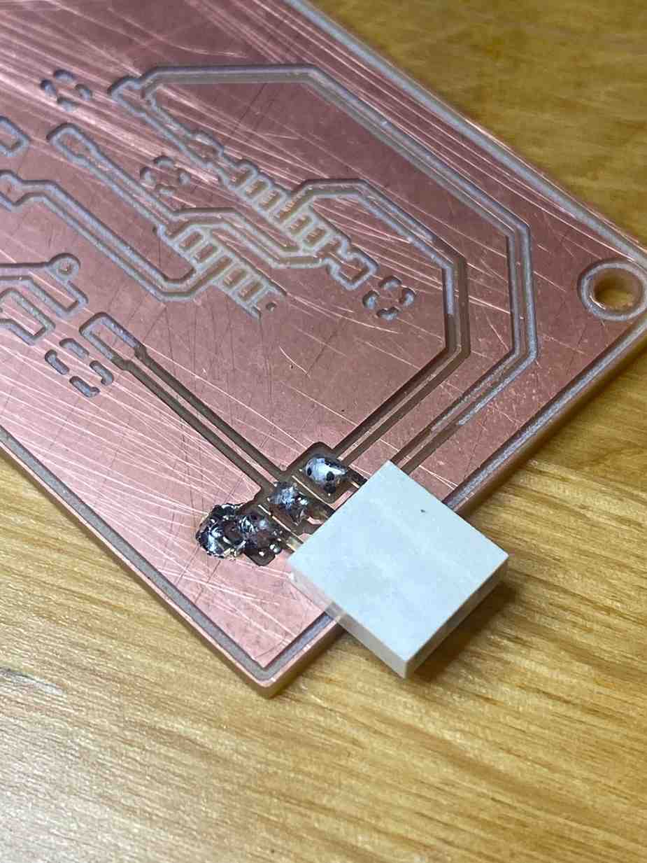
Fail #2 — Burning a trace
While fixing a joint, I overheated and ripped a copper trace entirely off the board.
This taught me:
- Don’t push down with the soldering iron
- Don’t reheat the same pad for too long
- Use flux instead of extra heat
Fail #3 — Milling defect
The SRM-20 didn’t mill certain traces deep enough.
This was not a soldering error but taught me to inspect milled traces carefully before starting soldering.
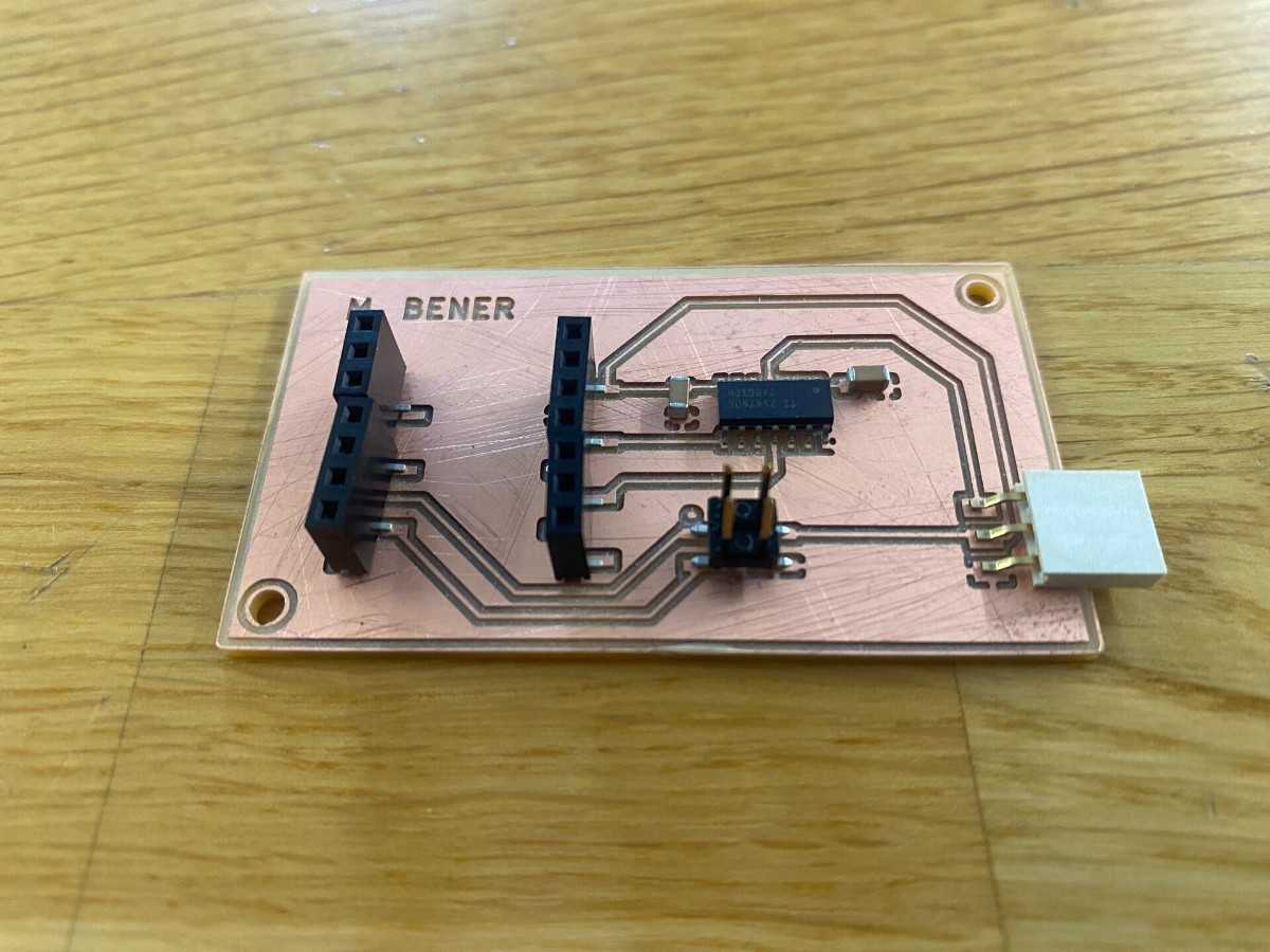
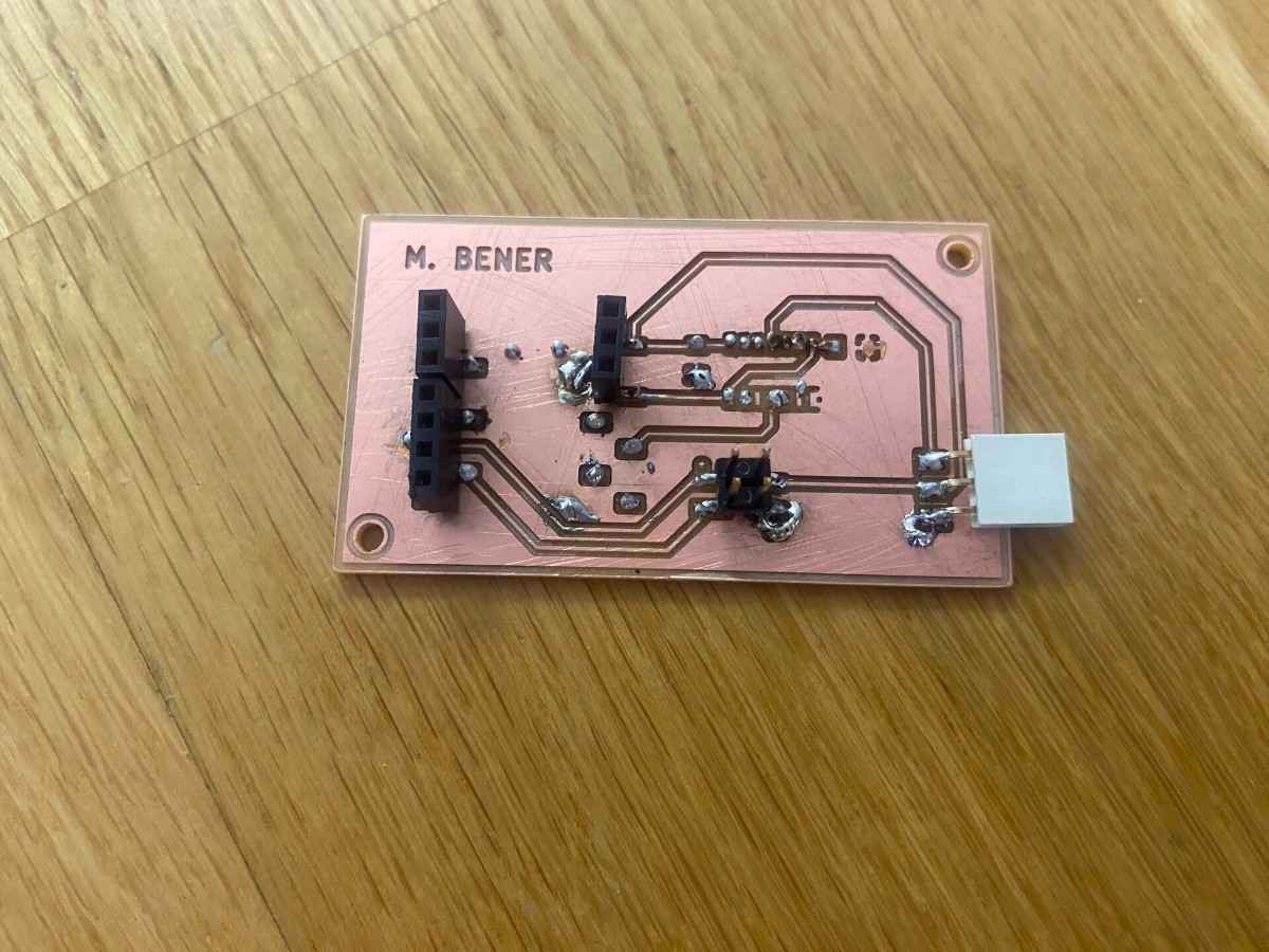
Final Working Board
After three failed boards, I used everything I learned to build a fully working board.
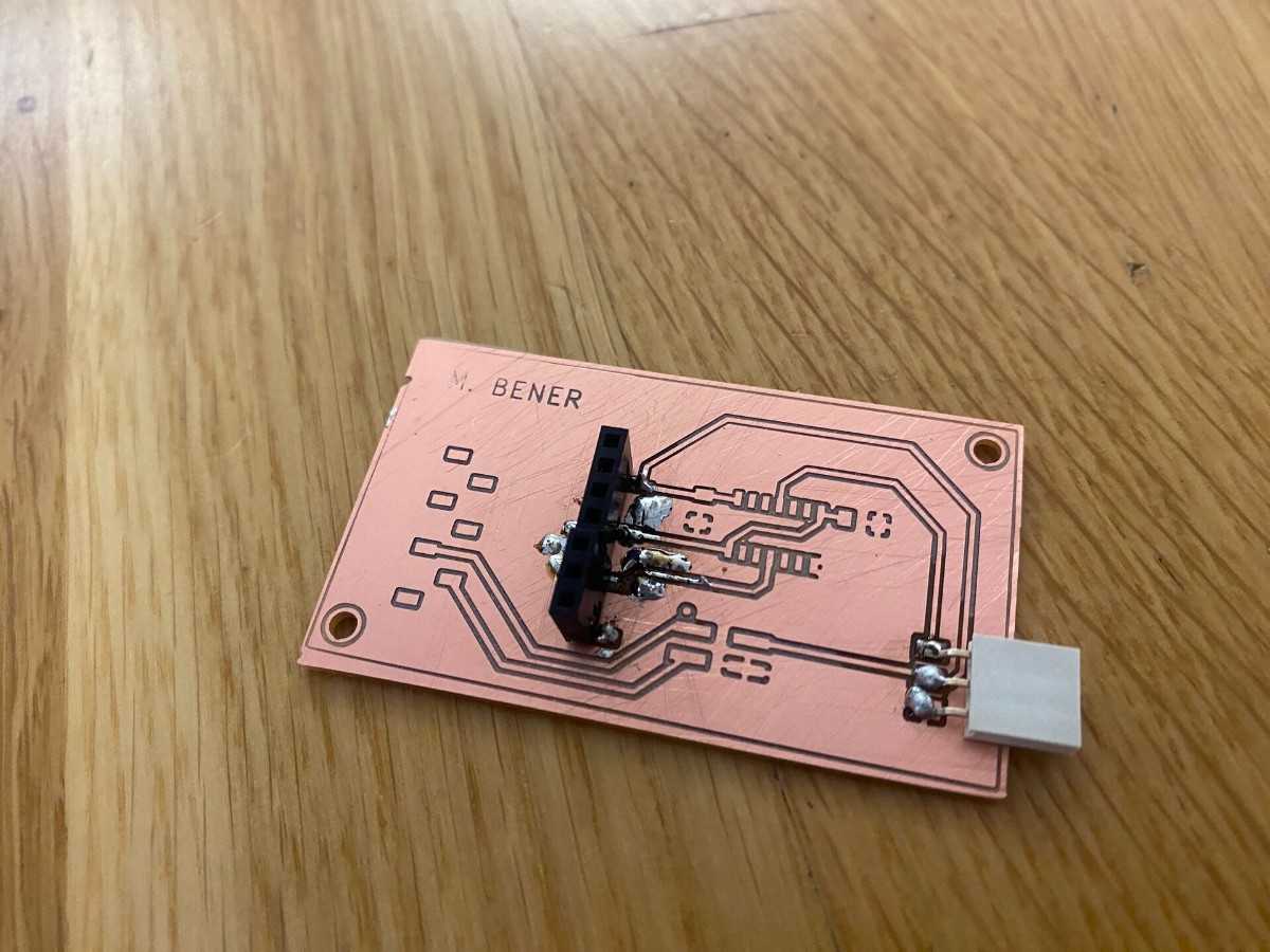
Board #4 — Soldering
However, I accidentally soldered the logic level shifter rotated 180°, mistaking the printed text orientation for the pin 1 marker.
I desoldered it using a hot air gun:
Note that while using a hot air gun be sure that there are not any flammable objects that can cause a fire due to the high heat coming from the hot air gun.
Some pads lifted during desoldering, but they belonged to unused pins, so the board was still salvageable.
Short Circuit Debugging
While testing, I discovered:
- A 5V pad was shorting through an isolated copper island connected by a capacitor
- ESP32 NC pins touching ground caused instability
I fixed both issues by removing excess solder.
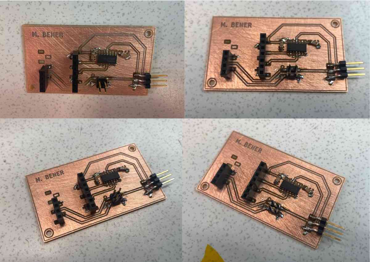
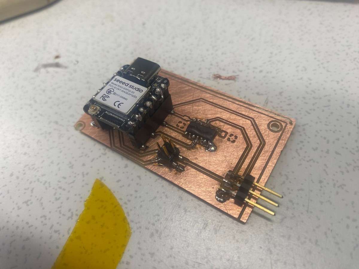
Final Working PCB (Hero)
The board now:
- Powers correctly
- Passes continuity checks
- Drives the servo motor
- Has no shorts or lifted critical traces
5. Reflection
This week was by far the most hands-on and failure-driven Fab Academy week so far.
I learned:
- PCB milling workflow end-to-end
- Proper handling of different drill sizes
- How fragile SMD pads are
- Why flux is mandatory
- How to desolder components safely
- Why orientation markers matter (pin 1 indicators!)
- How to find + fix short circuits with a multimeter
- How to keep calm through repeated failures
Across multiple failed boards, I built the confidence and skill to solder a fully working custom PCB from scratch.
This week made me feel like I finally understand the full electronics production pipeline—not just in theory, but in real physical practice.
6. Group Project
You can check our group project here