Introduction
For this week, I designed a simple PCB as a way to test the full electronics design workflow in KiCad, from schematic to a fabrication ready board.
Learning Outcomes
Select and use software for circuit board design: I used KiCad for schematic and PCB layout.
Demonstrate workflows used in circuit board design: I followed schematic → footprint assignment → PCB layout → routing → ERC/DRC → export.
Hero Shots
PCB Overview
The idea is that every time the button is pressed, the board generates a random color result (with different probabilities). If the rare “green” result appears, the board plays a short winning sound.
This allowed me to practice correct component selection, footprint assignment, routing, ground strategy, and ERC/DRC checking in a complete PCB design process.
Group Assignment
Group assignment page:
https://week-6-group-assignment-f3155c.fabcloud.io/
Software Used
KiCad (schematic + PCB layout)
Schematic Design
Creating the schematic
I started by creating the schematic in KiCad and organizing the board into simple blocks:
- Xiao ESP32-C3 module: main board
- Button input: Push button, Omron (SW1)
- RGB LED output: RGB CreeLed PLCC4 (D1)
- Speaker output: Buzzer (LS1)
- Resistors: 125,50,50 Ohm Resistors (R1, R2, R3) for the RGB LED channels
- Power: 3V3 and GND
I also:
Checked the datasheet of CRGB CreeLed PLCC4 as I was not sure if it was suitable for this project, even if it were, I did not know how it worked. https://downloads.cree-led.com/files/ds/h/HB-CLV1A-FKB.pdf . I learnt that it is a common anode rgb led which meant that a single power line was then distributed into 3 pins which are r,g,b. I have to remember this when doing the routing. This is a good example to check the datasheets of your components.
Resistor Calculations
At IF = 8mA:
- Red forward voltage ≈ 1.9V
- Green forward voltage ≈ 3.0V
- Blue forward voltage ≈ 3.0V
(Values from Led’s datasheet)
Since my board operates at 3.3V (ESP32-C3 supply), resistor values must be calculated using Ohm’s Law.
Formula used:
R = (Vsupply − Vforward) / I
Target current per channel: ~10mA
This keeps brightness strong while staying safely below maximum ratings.
Red Channel
R = (3.3V − 1.9V) / 0.01A
R = 1.4 / 0.01
R ≈ 140Ω
Closest value used: 125Ω
Green Channel
R = (3.3V − 3.0V) / 0.01A
R = 0.3 / 0.01
R ≈ 30Ω
Closest value used: 50Ω
Blue Channel
R = (3.3V − 3.0V) / 0.01A
R ≈ 30Ω
Closest value used: 50Ω
Final Resistor Values Used
Red 150Ω
Green 33Ω
Blue 33Ω
By calculating each resistor separately:
- Current is controlled properly
- Brightness between channels is more balanced
- The board behaves more predictably
- The design reflects correct practice
Assigning symbols and footprints
Once the schematic was complete in my head, I used Krisjanis Rijnieks’s KiCad FabLib for the symbols. (https://gitlab.fabcloud.org/pub/libraries/electronics/kicad) You can follow its instructions to add the library to KiCad. After adding symbols, we will then be working on the footprints of every component.
At this stage I learned an important lesson:
I initially added parts without checking whether those exact components exist in our lab, and also without confirming the correct variant.Because many components have multiple similar labels/versions, selecting the wrong one can result in:
- incorrect pad sizes
- assembly problems later
Fix: Before finalizing the PCB, I verified:
- that it has correct footprint
- the physical size of the part
- that the component is available in the lab
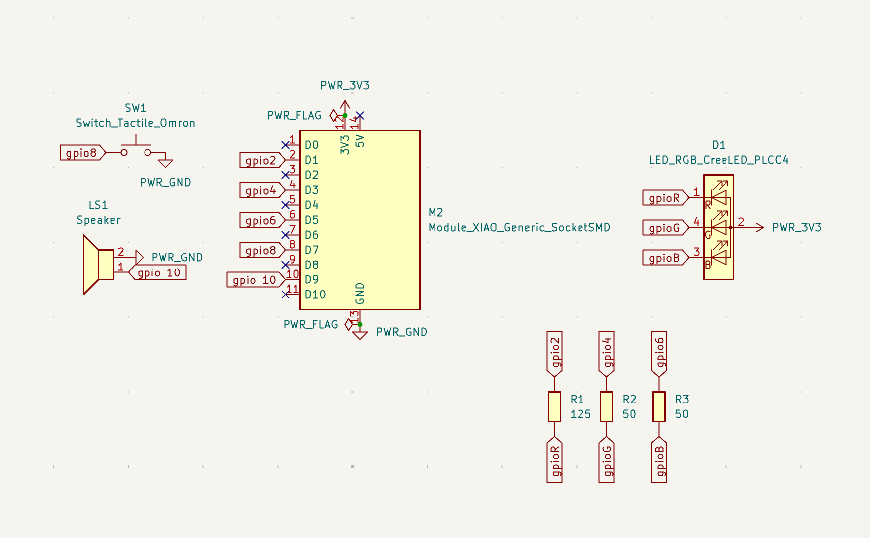
Schematic designed in KiCad.
ERC (Electrical Rules Check) + fixing power flag issue
After finishing the schematic, I ran ERC to catch design issues early before moving to PCB layout.
During ERC, I realized I had not added PWR_FLAG symbols, so KiCad treated the power nets as if they were not being driven properly.
This created ERC warnings and made it clear that I should fix power handling before continuing.
Fix: I added the missing PWR_FLAG symbols and re-ran ERC to confirm the schematic was clean.
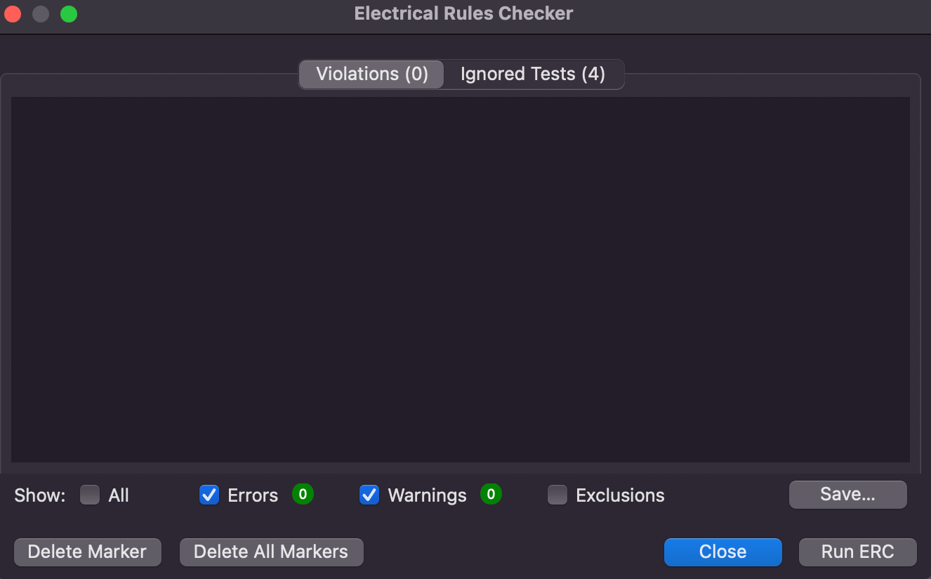
ERC tool giving no error.
PCB Editor (Placement + Routing)
Creating the board outline
After importing the design into the PCB editor, I first drew the board outline:
- Outline layer: Edge.Cuts
- Rounded corners for a clean shape
This step defined the final physical limits of the PCB and helped keep placement organized.
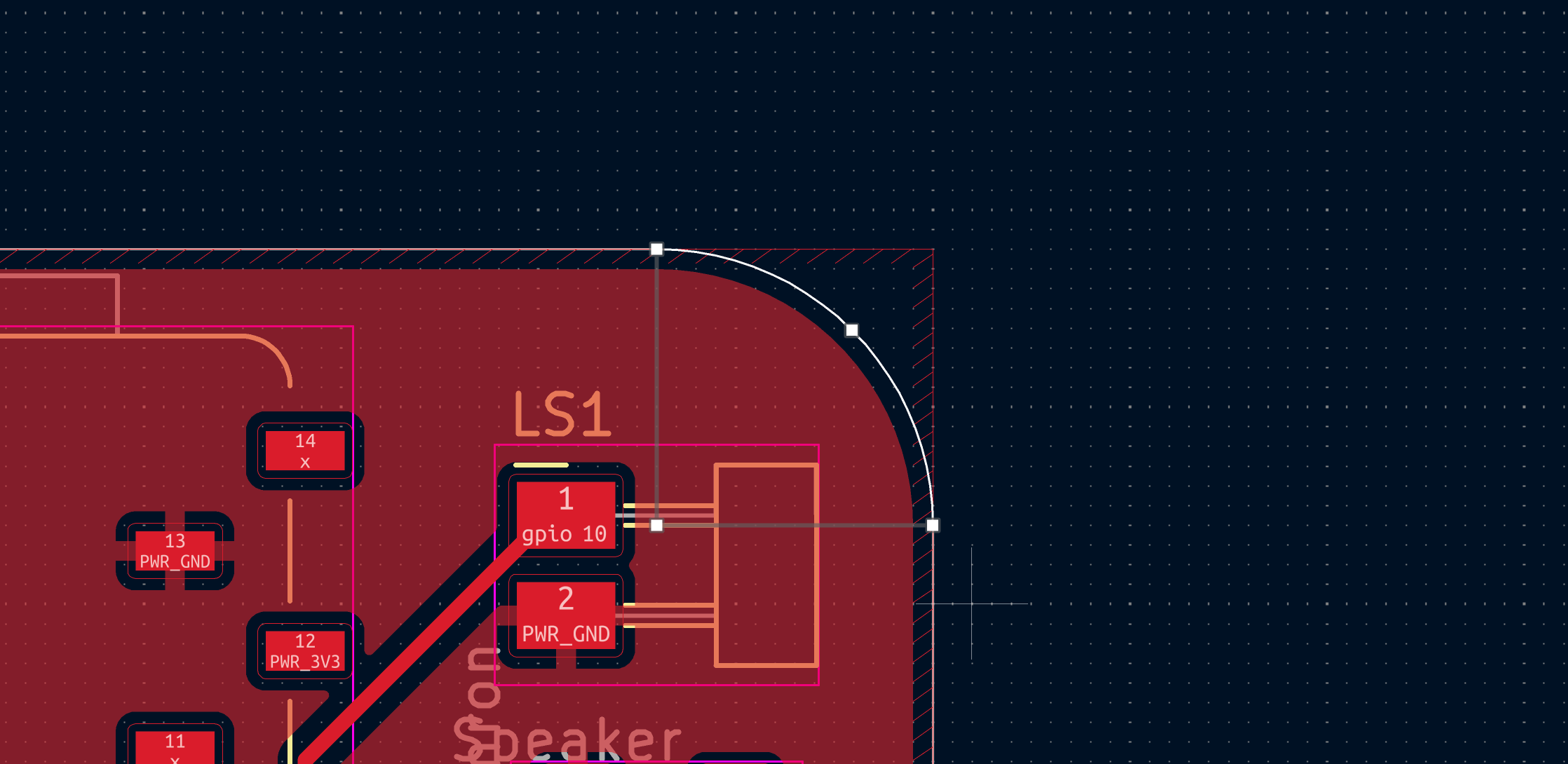
Example for a rounded edge cut.
Component placement
Before drawing connections, I placed components carefully to make routing easier.
Placement decisions:
- ESP32-C3 near the center (main controller)
- SW1 (button) near the edge (easy access)
- D1 (RGB LED) placed clearly visible
- R1/R2/R3 placed close to the LED to keep traces short
- LS1 (speaker) placed to avoid long, messy traces
I also left enough space for soldering and avoided placing components too close together.
Routing (drawing copper connections)
After placement, I began routing the connections based on the schematic nets in F.Cu layer.
Trace width
I used a 0.4 mm trace width for routing.
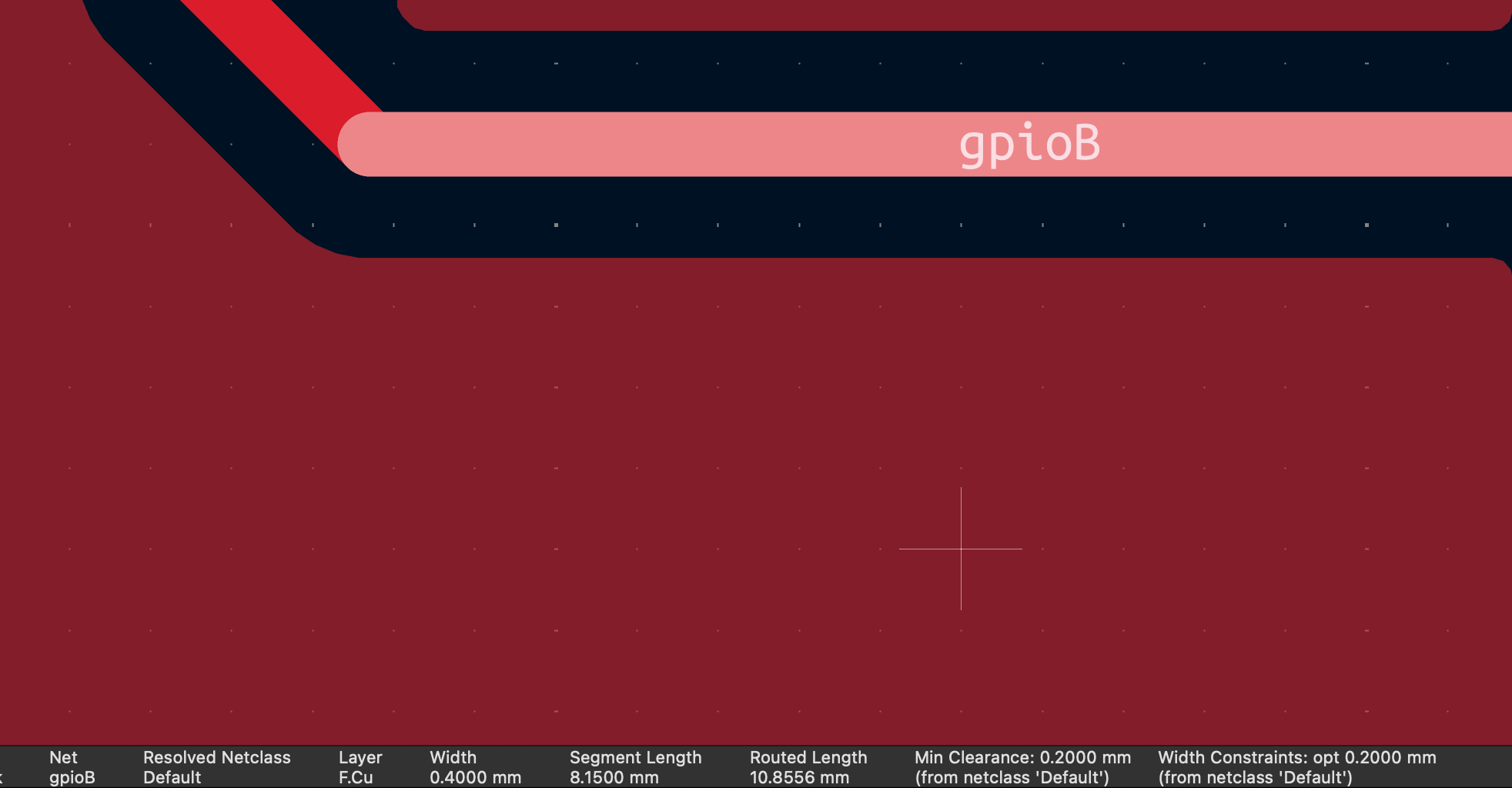
Figure 4 — 0.4mm trace
Routing approach
While routing I focused on:
- short, direct signal paths
- avoiding unnecessary bends
- making the PCB readable
- minimizing crossings
- NO 90 DEGREE ANGLES (Results in incostistent lines in the production.)
Ground plane (GND all over the board)
Instead of manually routing every single ground connection, I used a GND copper fill.
This made ground available across most of the PCB and gave me these advantages:
- cleaner routing (less manual GND traces)
- easier connections to ground pins
- more stable board reference
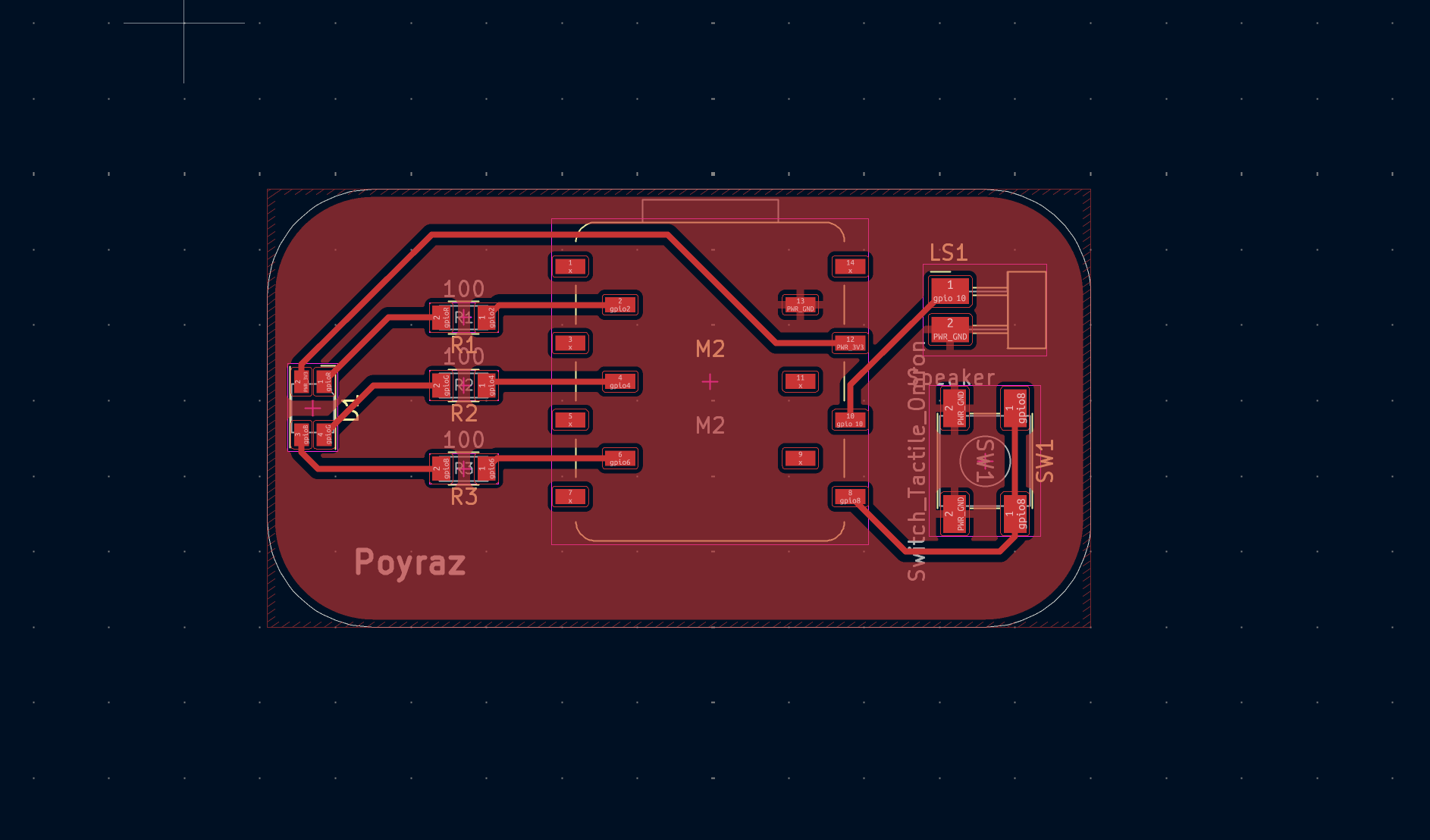
PCB layout screenshot
PCB layout view showing placement, routing, and ground fill.
DRC and Fabrication Readiness
DRC (Design Rules Check)
After completing routing and ground filling, I ran DRC to verify that the board can be fabricated.
This confirmed:
- no shorts
- no clearance issues
- all nets routed correctly
- board outline is correct
Passing DRC gave confidence that the PCB is fabrication ready.
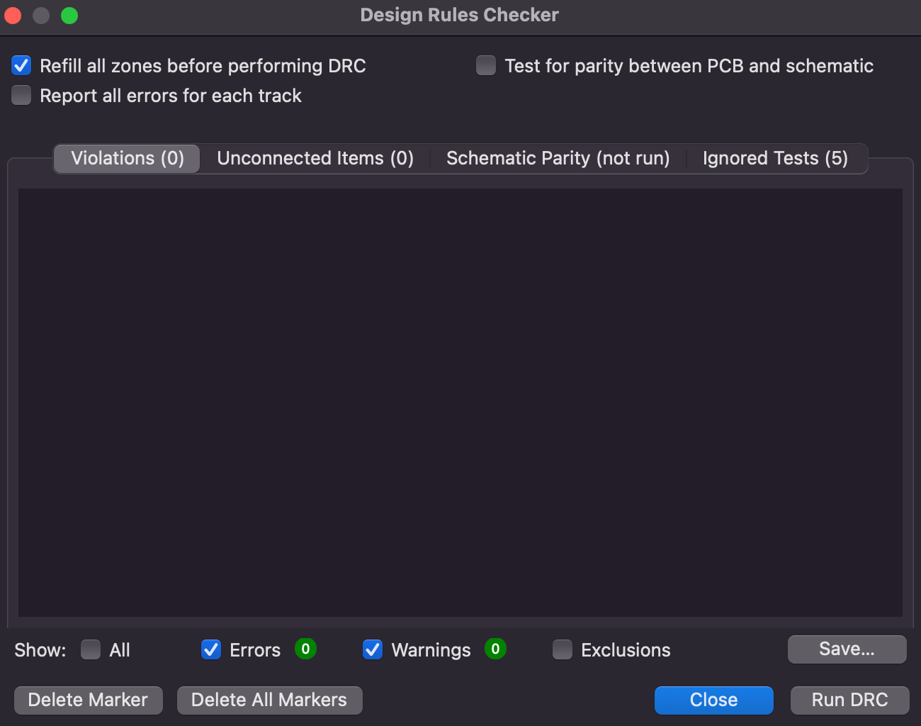
DRC tool showing no error.
Exporting the manufacturing files
Finally, I exported:
SVG files
These files are not the standard outputs needed for PCB fabrication. Gerber files are mainly used but since I am new to this process, using svg is easier.
Reflection (What I Learned)
This week helped me understand that electronics design is not only connecting components, but also verifying the design step-by-step.
Key takeaways:
- ERC helped me catch missing PWR_FLAG issues early
- footprint selection must match real available components
- component placement affects routing quality a lot
- using a GND plane makes the PCB cleaner and easier to route
- DRC is necessary to confirm fabrication readiness
Result: A complete KiCad PCB design with 0.4 mm routing, ground plane filling, ERC/DRC verification, and fabrication-ready exports.
Files
I included the original KiCad project files so the board can be edited or reproduced: Download the designs