Introduction
This week focused on electronics production: preparing manufacturing files, generating toolpaths, milling the PCB, soldering the components, debugging the board, and programming it.
For this assignment, I produced the same microcontroller development board that I designed in Week 06 and tested that it works by successfully uploading a program to it.
Group Assignment
Group assignment page:
Tools and Materials
Hardware
- Roland SRM-20
- FR1 copper board
- 0.4 mm v-bit mill for traces
- 2mm end mill for outline
- Soldering iron
- Solder and flux
- Multimeter
Software
- KiCad
- Inkscape
- Mods
- Roland Software
- Arduino IDE
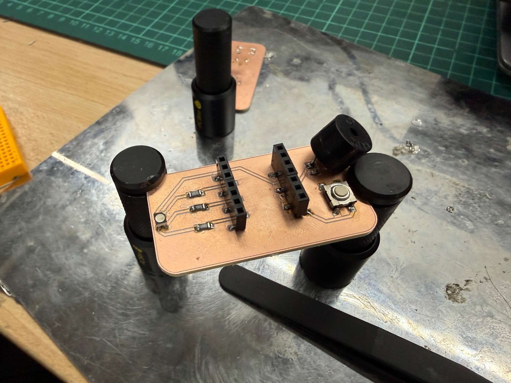
Hero Shot
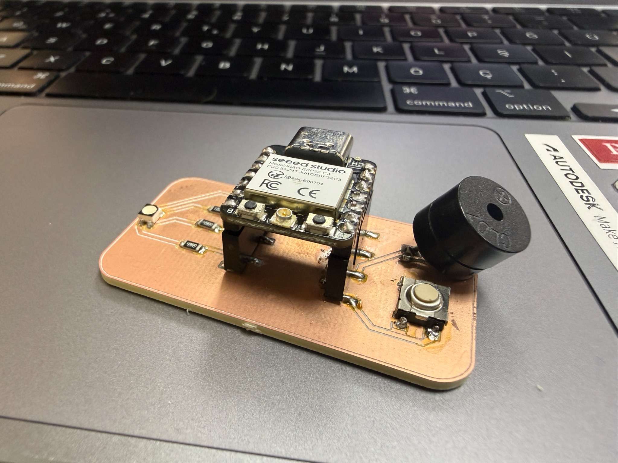
Board Overview
The PCB I produced this week is the microcontroller board I designed in Week 06.
Main features of the board:
- ESP32-C3 microcontroller
- button input
- RGB LED output
- buzzer output
When the button is pressed, there will be a random generated color (r,g,b) with green having a low possibilty of 15%. When green occurs, there is a winning sound.
This week was focused on manufacturing the board correctly and verifying that it works in practice.
Preparing the Manufacturing Files
Exporting from KiCad
I started by exporting the required PCB layers from KiCad.
The two main files I needed were:
- the copper traces
- the board outline from Edge.Cuts
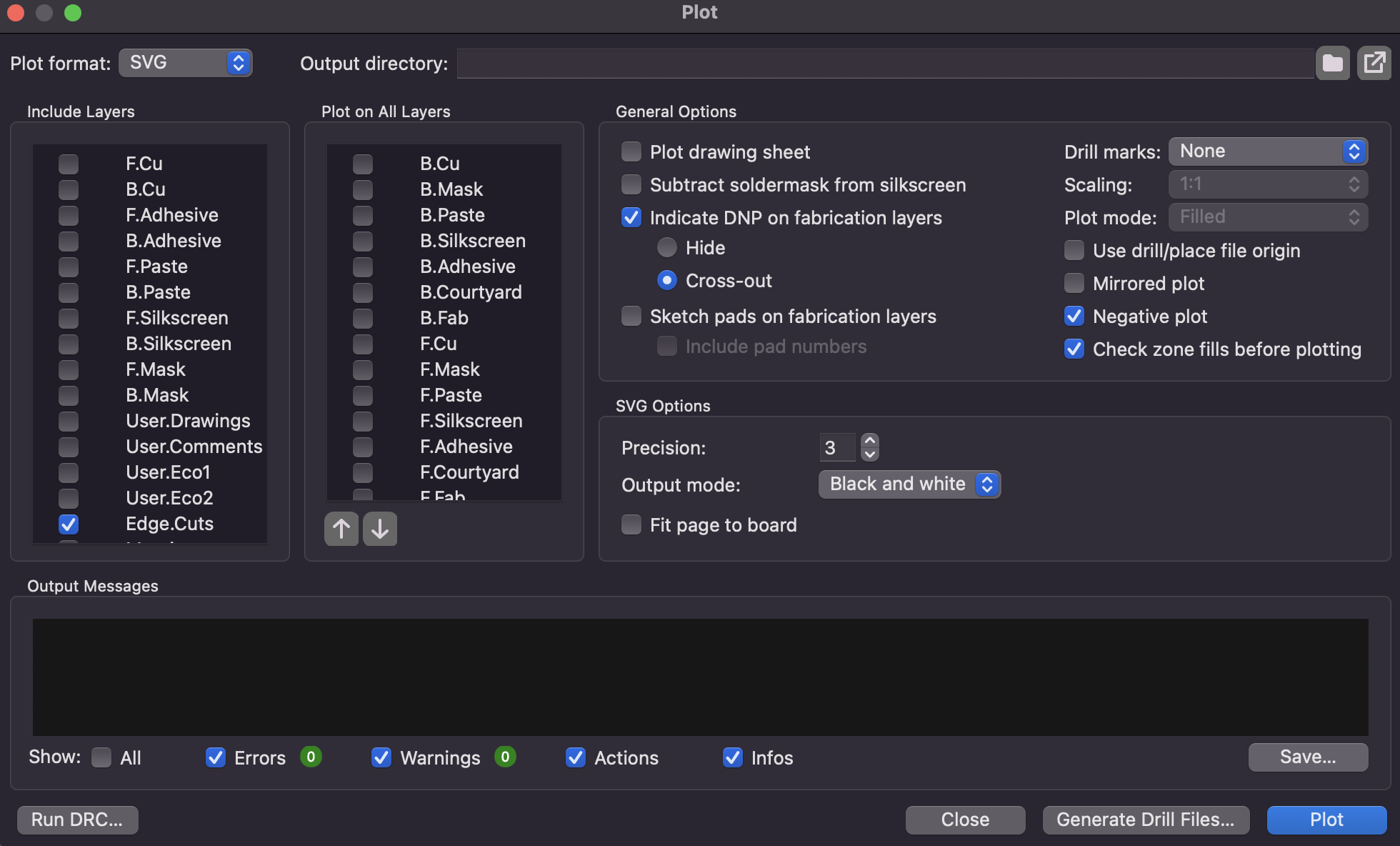
Preparing the files for Mods
After exporting the design files, I prepared them through Inkscape so they could be used correctly in Mods for PCB milling.
For the traces file, I made sure that the areas to be milled were clearly defined.
For the outline file, I had to prepare the image carefully so that Mods could read the cut correctly. The cut boundary had to be visible as a proper black shape, while the non-cut area remained white. I initally had problems with creating a white object inside the edge cuts, don’t forget to combine all parts, and then press shift+j to connect unconnected nodes.
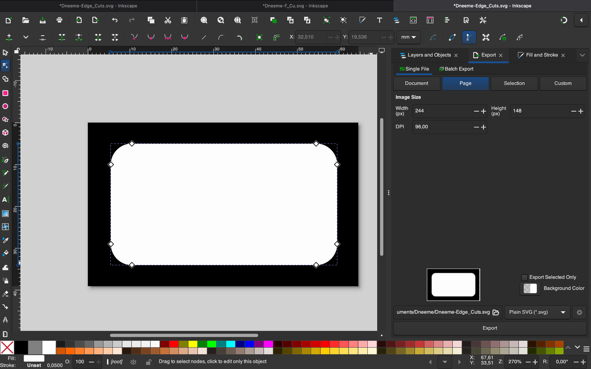
This little thing would have saved me couple of hours because I was forcing mods to read that .svg without any infill and it wasn’t generating any toolpaths at all.
After fixing it i also checked:
- canvas size
- scale
To orient the traces and edge cut easier while cutting.
Toolpath Generation
Trace toolpath
I used Mods with the Roland SRM-20 milling workflow to generate the trace toolpath. I imported .svg files that i got from Inkscape.
Settings used for traces:
- tool diameter: 0.4 mm
- cut depth: 0.10 mm
- max depth: 0.10 mm
- offsets: 1
(there is a v-bit calculator which makes it easier)
Outline toolpath
After generating the traces, I prepared the toolpath for cutting the board outline.
Settings used for the outline:
- tool diameter: 2 mm
- cut depth: 0.60 mm
- max depth: about 1.8 mm
- offsets: 1
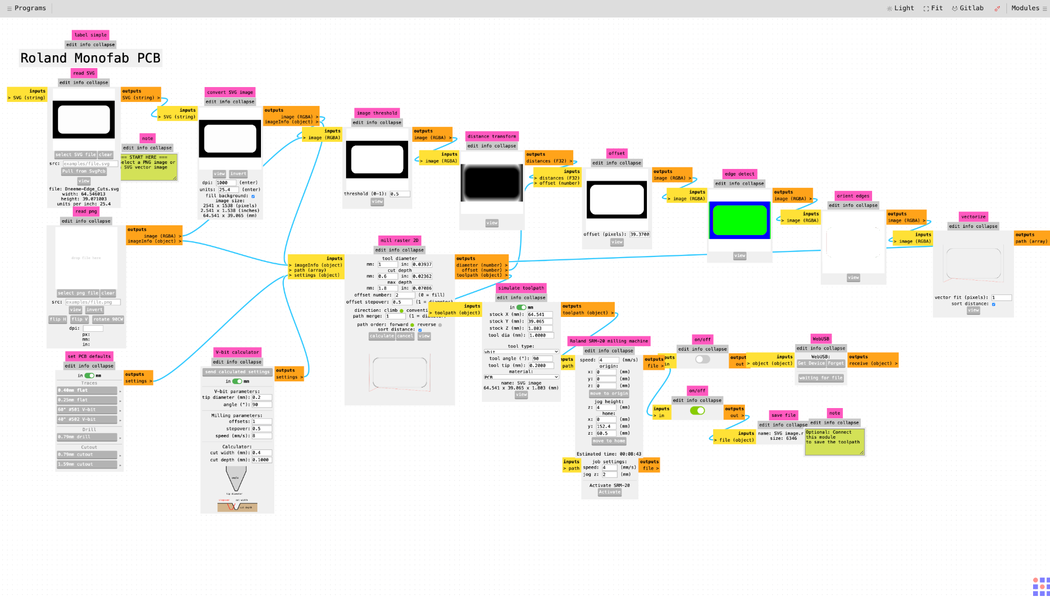
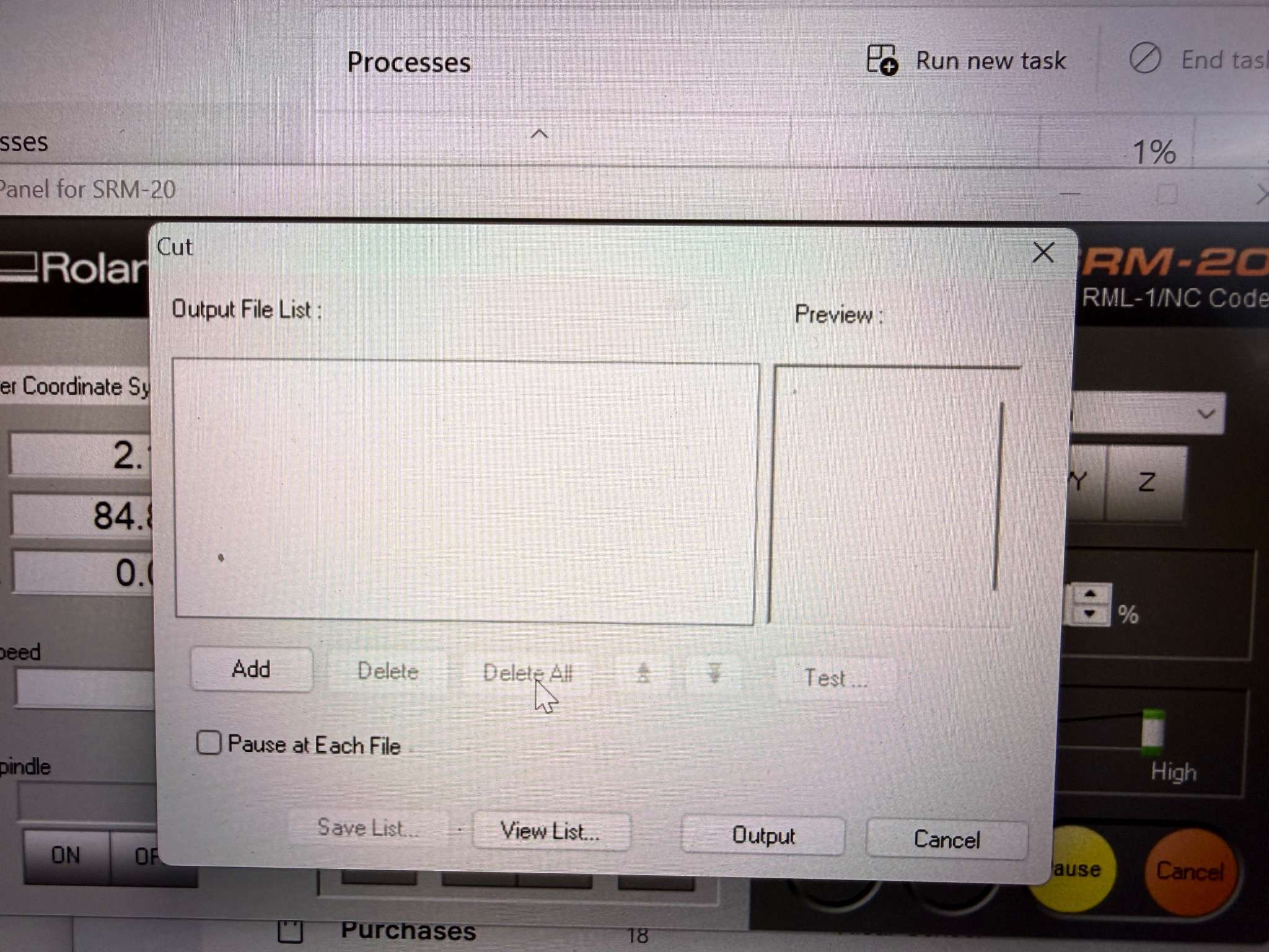
Both processes gave .rml file which are toolpaths for the milling process through SRM-20.
Milling Process
Fixing the board on the bed
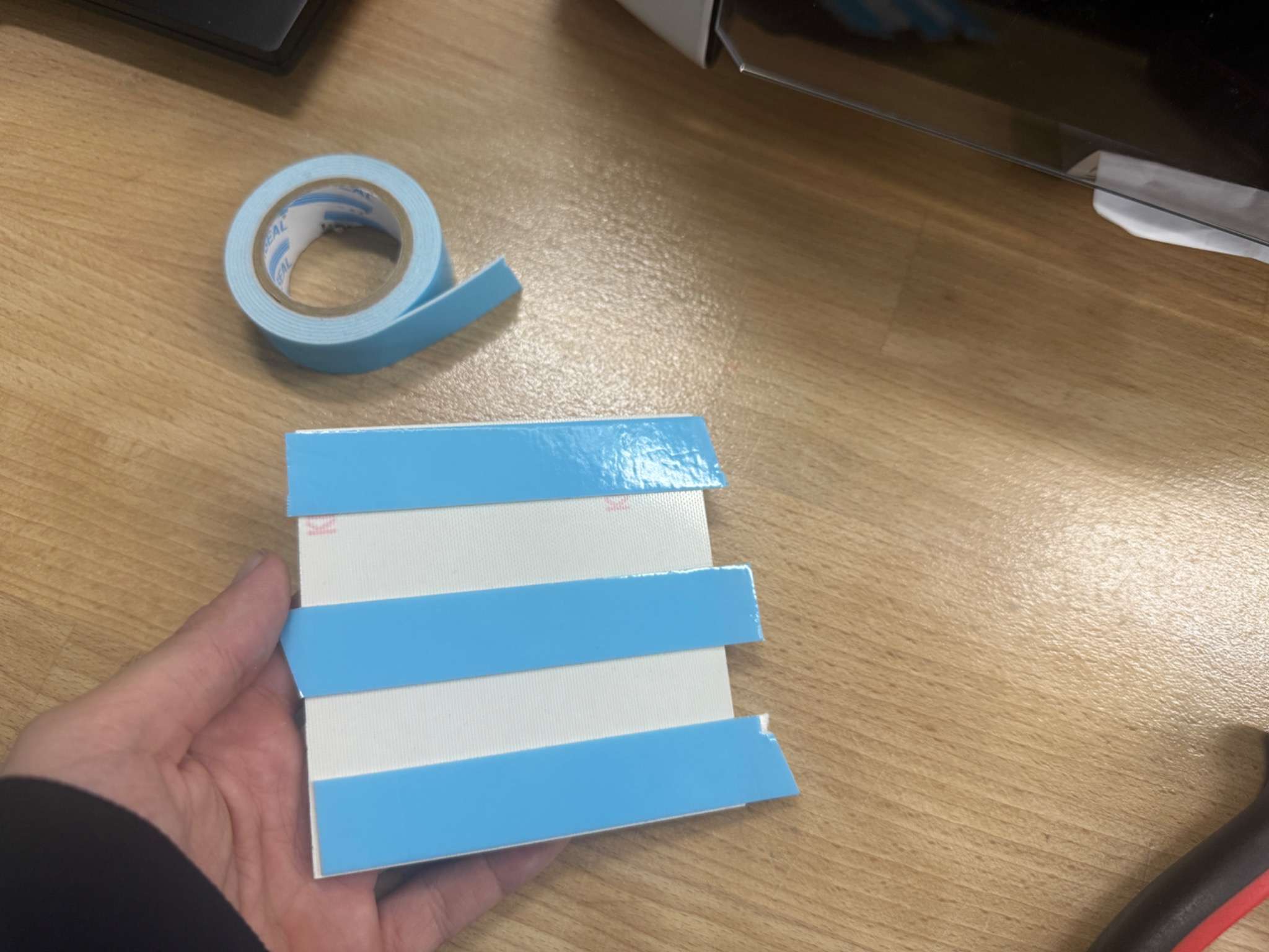
I used double-sided tape to attach the FR1 board securely to the milling bed so that it would not shift during cutting.
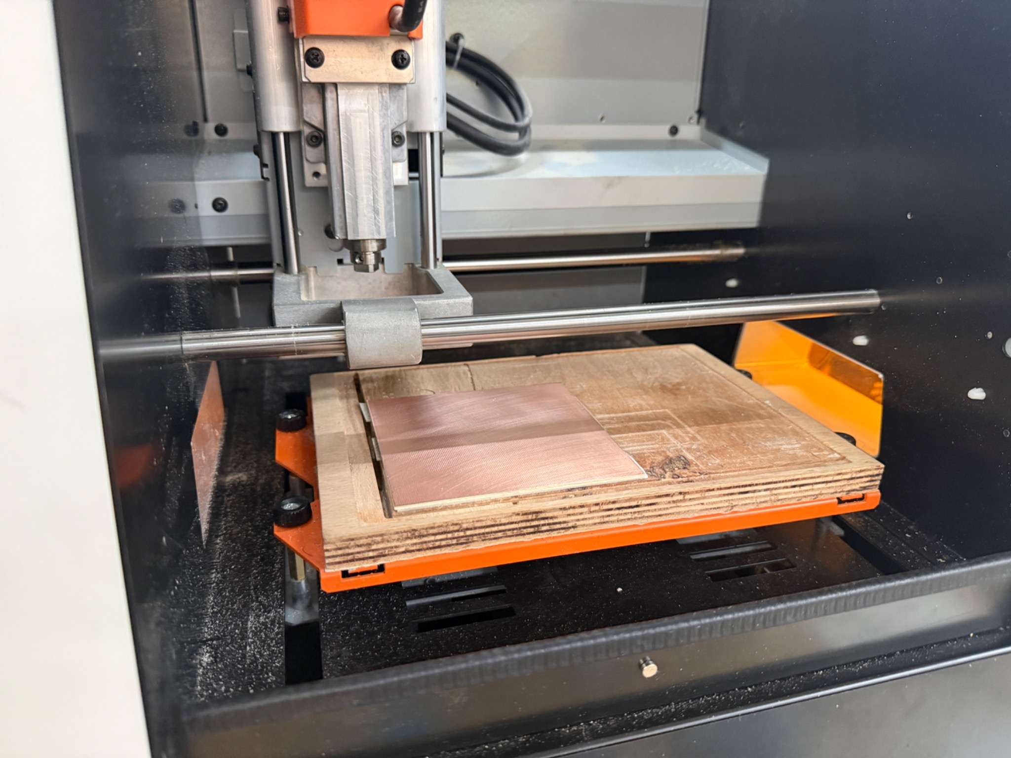
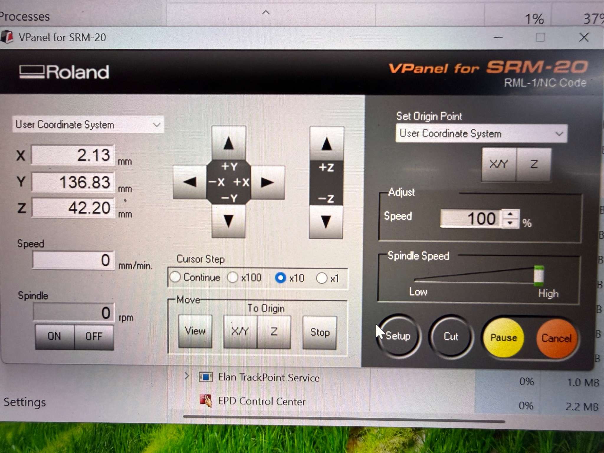
Setting the origin
In VPanel, I set the X, Y, and Z origin carefully:
- X and Y at the corner of the work area
- Z on the copper surface (be careful not to break the bit)
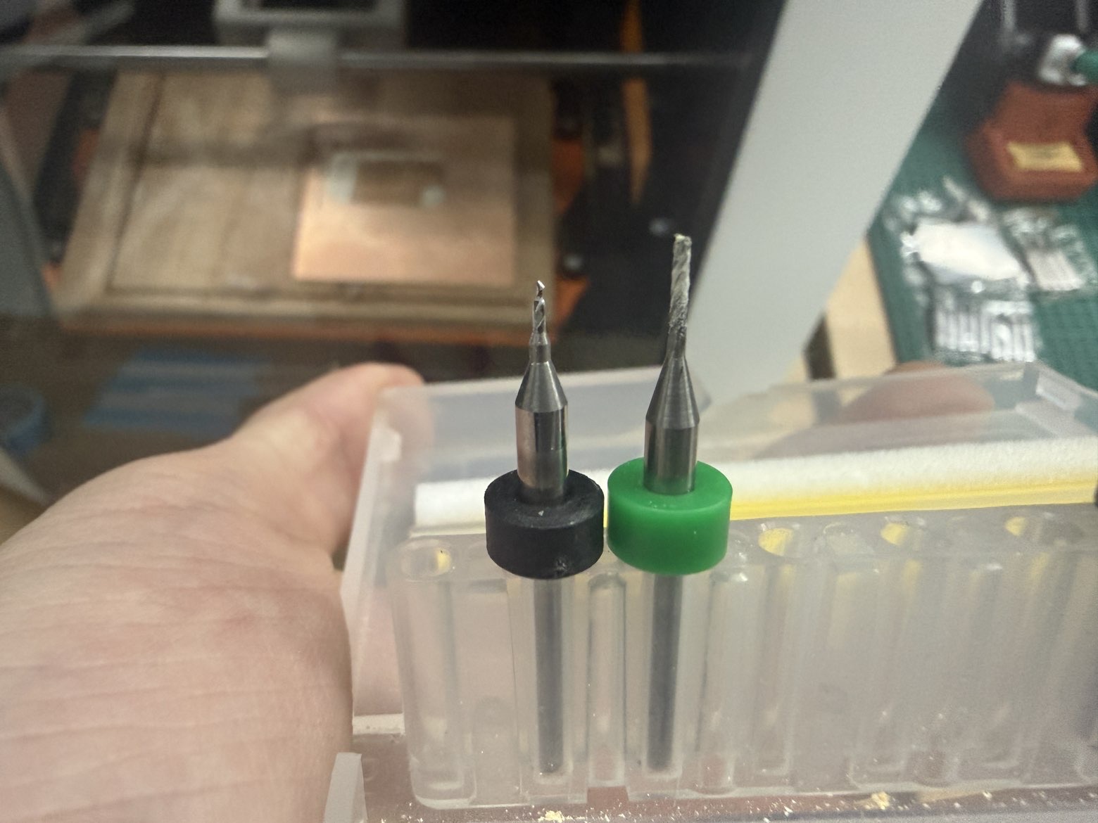
Bits
I milled the board in two stages:
- traces with the 0.4 mm v-bit
- outline with the 2 mm bit
Cutting
To cut your PCB, press the cut button on the software and uplad your traces first then edge cut since its healthier to get traces in a more stable plane. Press cut and the machine starts to work according to the .rml files.
First milling attempt
My first attempt failed because I did not properly consider the reachable movement area of the SRM-20.
As a result, part of the PCB was placed outside the machine’s working area, so only part of the design was milled.
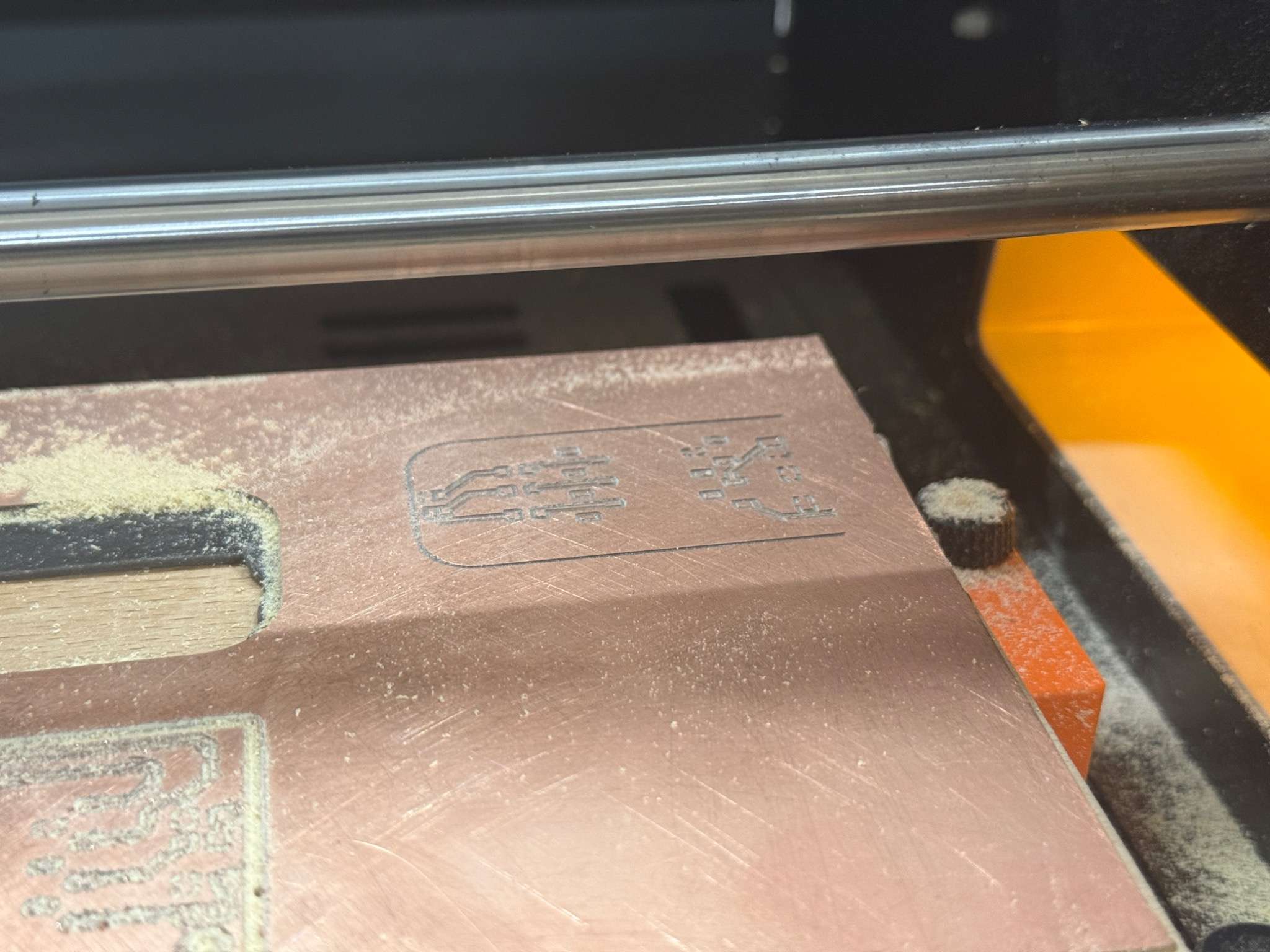
Second milling attempt
My second attempt also failed, but for a different reason.
This time, the board surface got scratched during movement because the jogging height was not set properly. The tool moved across the PCB without lifting high enough, which damaged the copper surface.
To solve this, I corrected the jogging height value in Mods so the bit would travel safely above the board between paths.
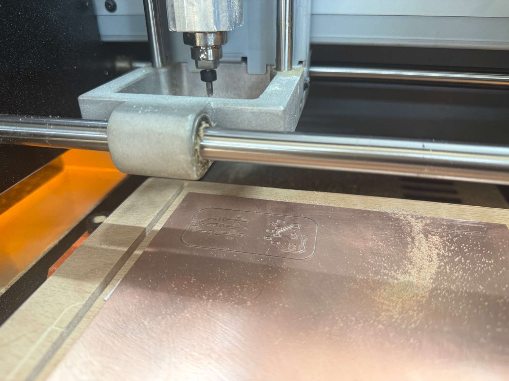
Final successful milling
After fixing the placement and jogging settings, I prepared the board again and repeated the milling process.
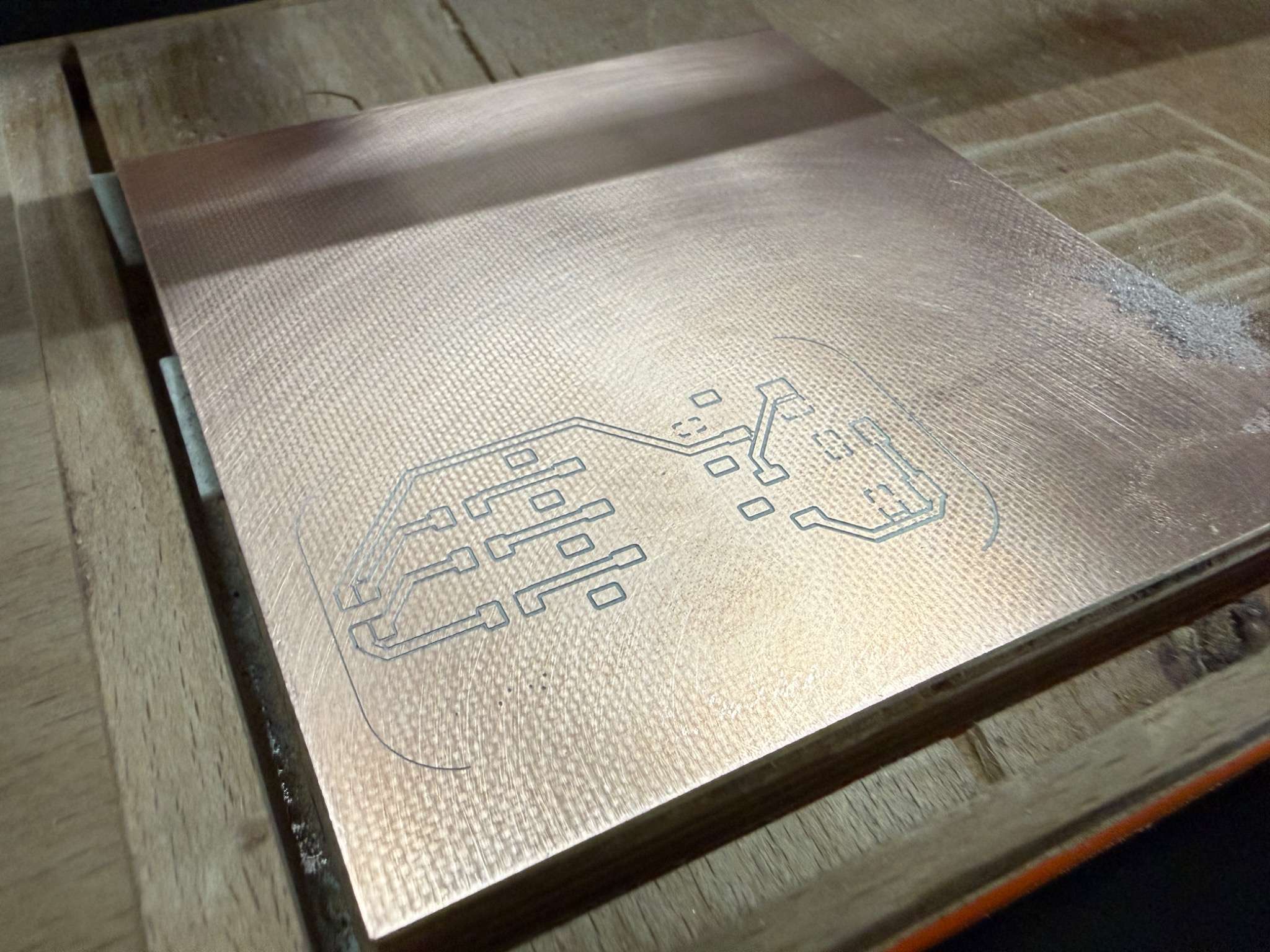
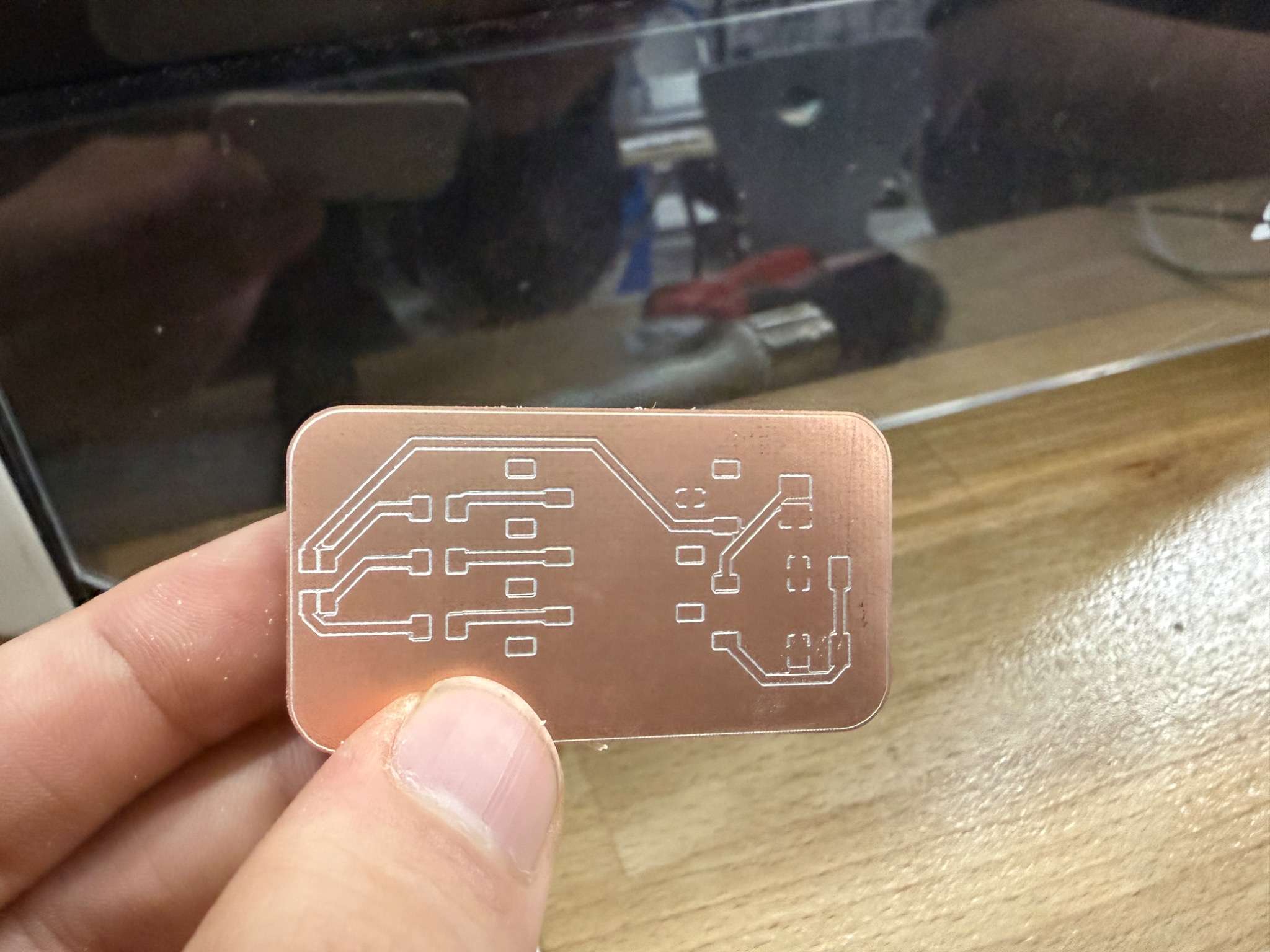
Final milled board
After milling, I cleaned the surface and checked the overall quality of the result.
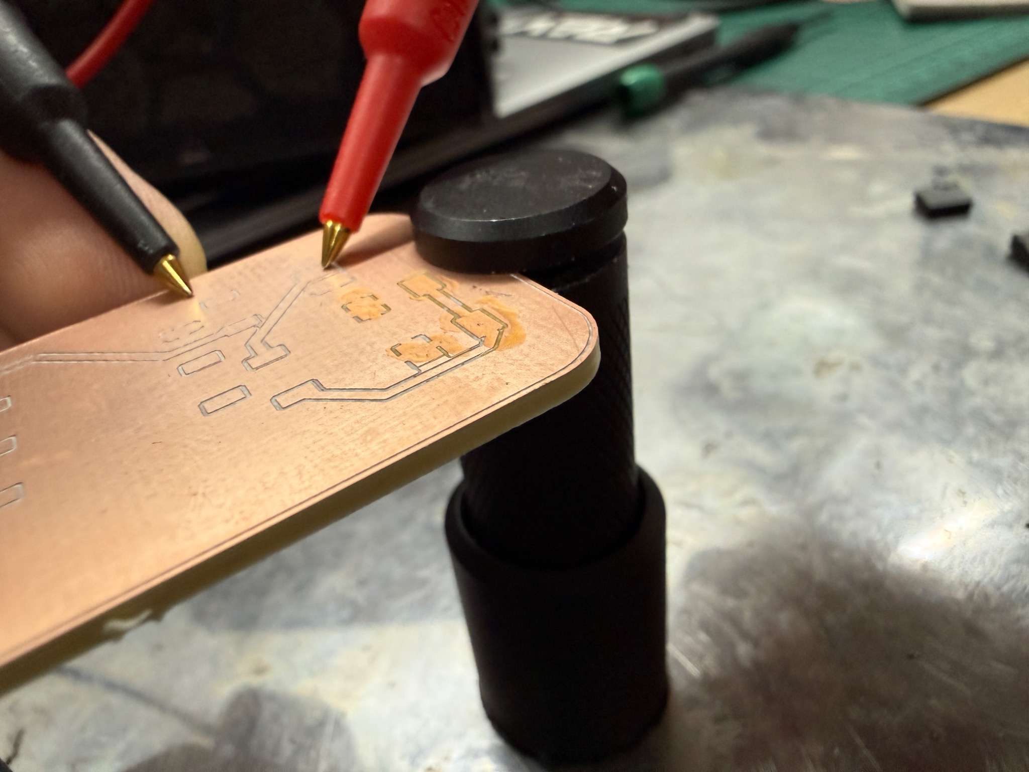
Pre-Soldering Checks
Before soldering, I checked the board with a multimeter.
I verified:
- that there was no short circuit between 3V3 and GND
- that important traces were electrically connected where expected
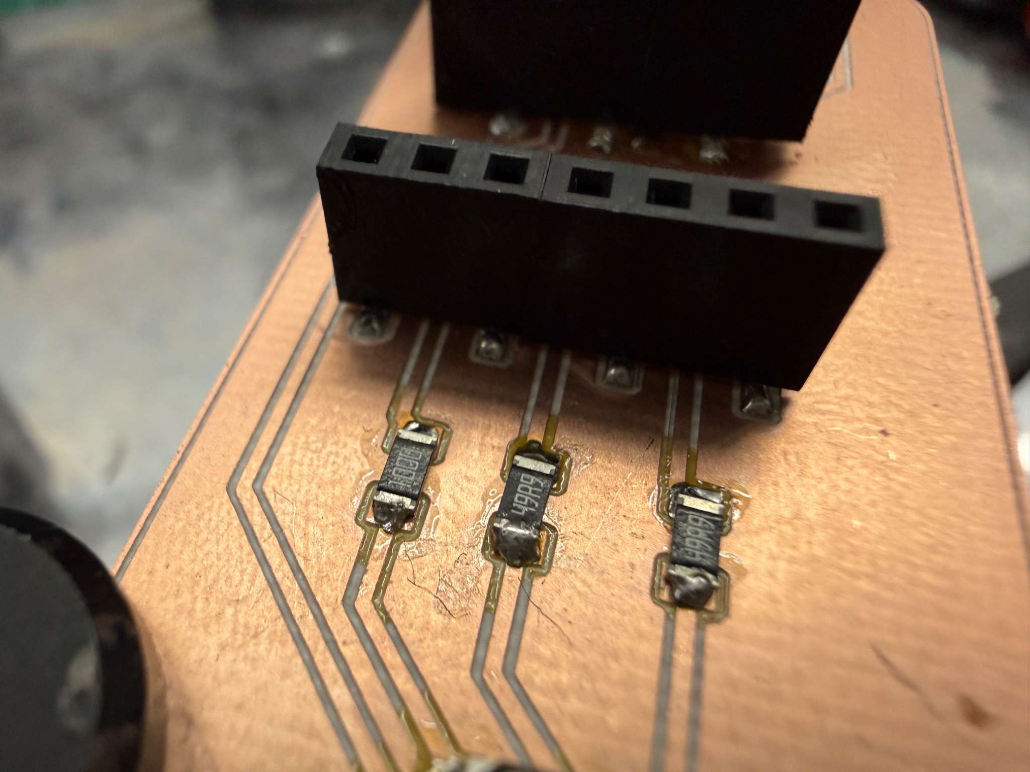
Stuffing and Soldering
Components used
The main components I soldered onto the board were:
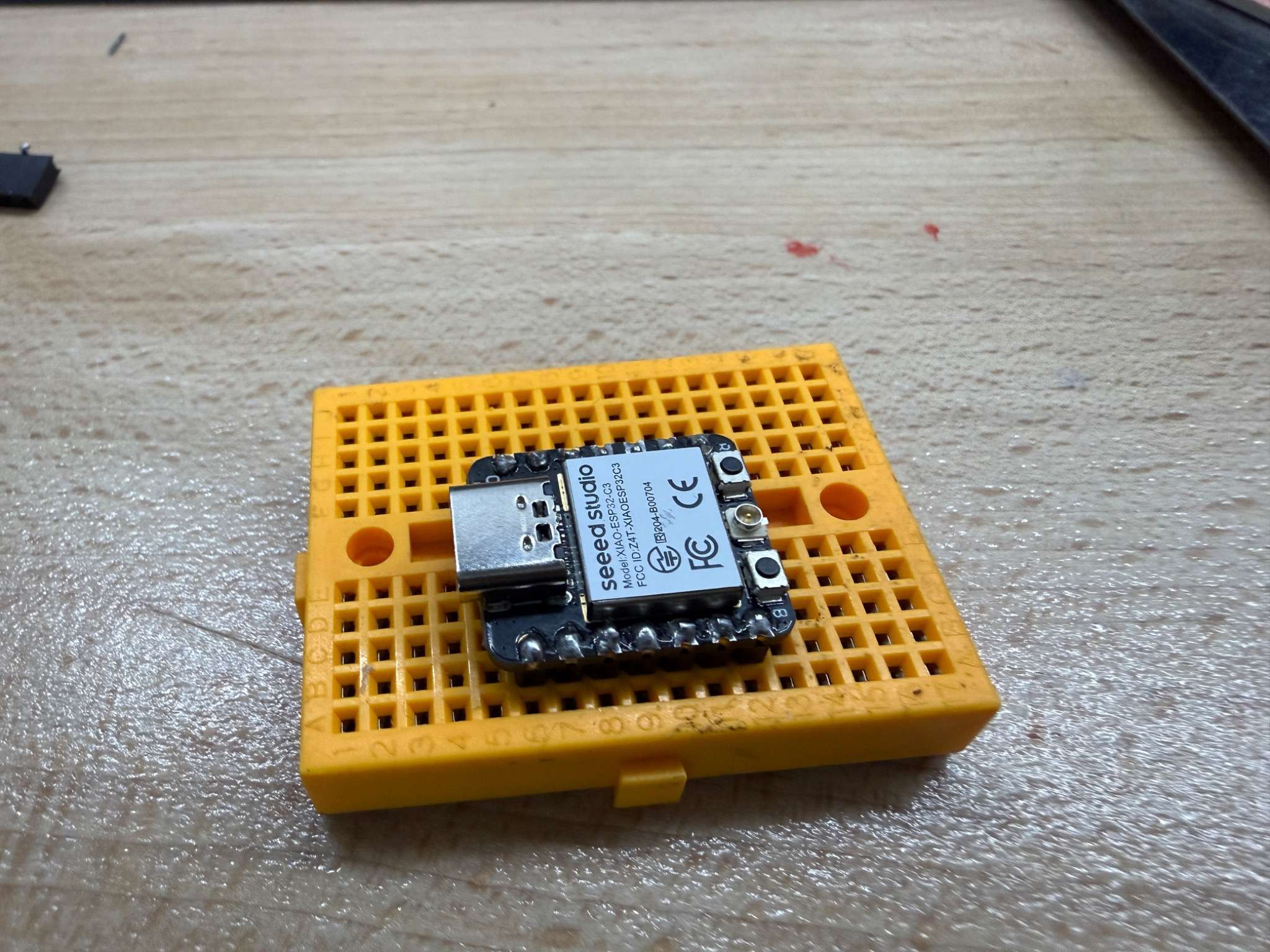
- Xiao ESP32-C3 module
- RGB LED
- resistors for the LED channels
- button
- buzzer
- headers if needed
Soldering process
I soldered the smaller components first and then moved to the larger parts. This made the assembly process easier and reduced the chance of accidentally blocking access to smaller pads.
My general order was:
- ESP32-C3 module and headers
- RGB LED
- button
- buzzer
- resistors
Debugging and Testing
Visual inspection
After soldering, I visually inspected the board to identify any obvious assembly problems.
I checked for:
- solder bridges
- cold joints
- misaligned components
- missing connections
And then checked it again with a multimeter.
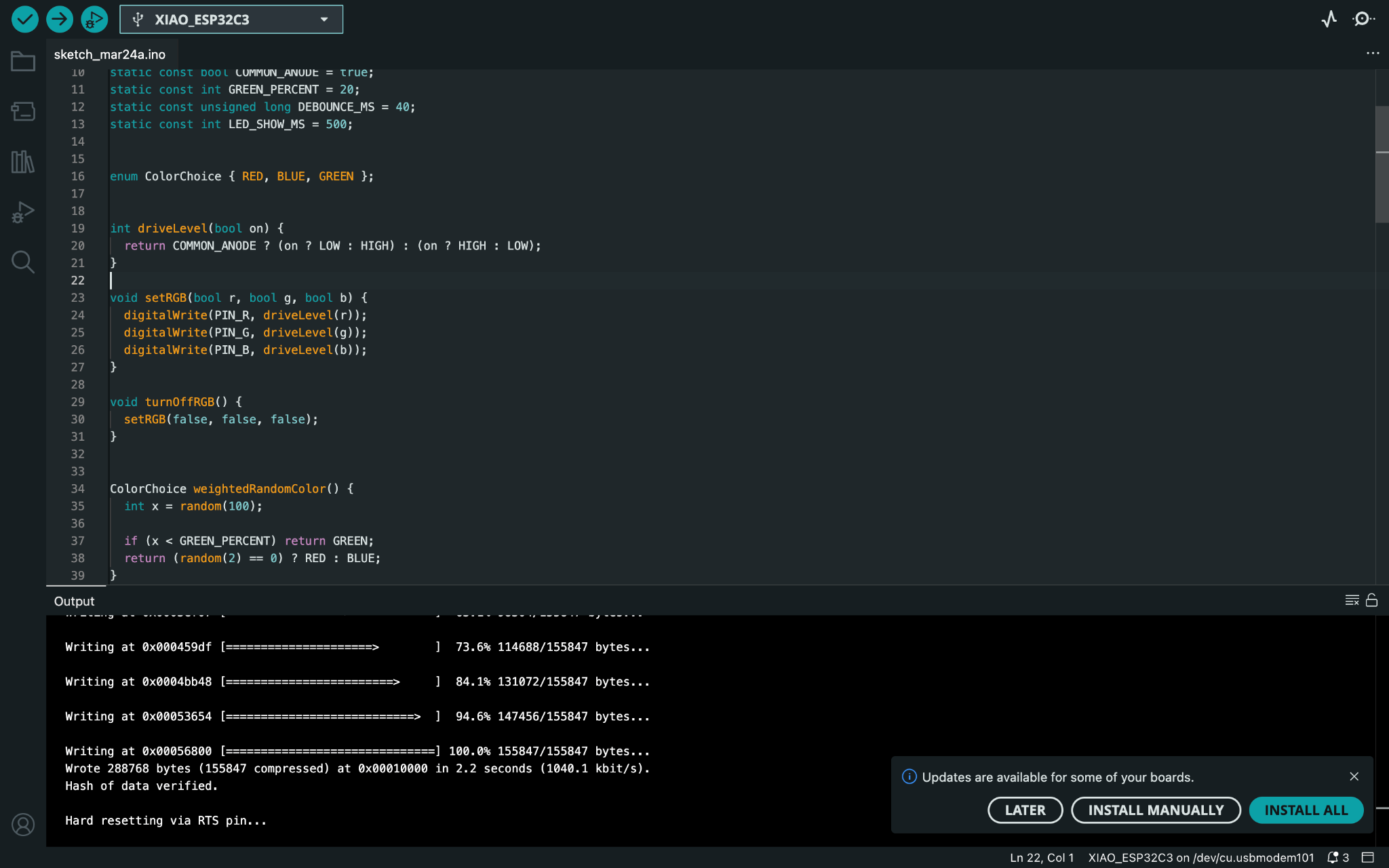
Functional test
To verify that the board works, I connected it and uploaded a test program to the ESP32-C3.
The successful upload confirmed that:
- the board could be powered correctly
- the microcontroller could be recognized and programmed
- the board was functional as a development board
Here is a video:
Programming
I used Arduino IDE to upload a test program to the board.
static const int PIN_R   = D1;
static const int PIN_G   = D3;
static const int PIN_B   = D5;

static const int PIN_BTN = D7;
static const int PIN_BUZ = D9;


static const bool COMMON_ANODE = true;
static const int GREEN_PERCENT = 20;
static const unsigned long DEBOUNCE_MS = 40;
static const int LED_SHOW_MS = 500;


enum ColorChoice { RED, BLUE, GREEN };


int driveLevel(bool on) {
  return COMMON_ANODE ? (on ? LOW : HIGH) : (on ? HIGH : LOW);
}

void setRGB(bool r, bool g, bool b) {
  digitalWrite(PIN_R, driveLevel(r));
  digitalWrite(PIN_G, driveLevel(g));
  digitalWrite(PIN_B, driveLevel(b));
}

void turnOffRGB() {
  setRGB(false, false, false);
}


ColorChoice weightedRandomColor() {
  int x = random(100);

  if (x < GREEN_PERCENT) return GREEN;
  return (random(2) == 0) ? RED : BLUE;
}


void losingSound() {
  tone(PIN_BUZ, 700, 120);
  delay(140);
  tone(PIN_BUZ, 500, 180);
  delay(220);
  noTone(PIN_BUZ);
}

void winningSound() {
  tone(PIN_BUZ, 700, 120);
  delay(140);
  tone(PIN_BUZ, 1000, 120);
  delay(140);
  tone(PIN_BUZ, 1400, 150);
  delay(170);
  tone(PIN_BUZ, 1800, 220);
  delay(250);
  noTone(PIN_BUZ);
}


void doEvent() {
  ColorChoice c = weightedRandomColor();

  if (c == RED) {
    Serial.println("RED - lose");
    setRGB(true, false, false);
    losingSound();
  }
  else if (c == BLUE) {
    Serial.println("BLUE - lose");
    setRGB(false, false, true);
    losingSound();
  }
  else {
    Serial.println("GREEN - WIN!");
    setRGB(false, true, false);
    winningSound();
  }

  delay(LED_SHOW_MS);
  turnOffRGB();
}


void setup() {
  Serial.begin(115200);
  delay(300);

  pinMode(PIN_R, OUTPUT);
  pinMode(PIN_G, OUTPUT);
  pinMode(PIN_B, OUTPUT);

  pinMode(PIN_BTN, INPUT_PULLUP);
  pinMode(PIN_BUZ, OUTPUT);

  turnOffRGB();
  digitalWrite(PIN_BUZ, LOW);

  randomSeed((uint32_t)esp_random());

  Serial.println("System ready.");
  Serial.println("Press the button.");
}


void loop() {
  static int lastReading = HIGH;
  static int stableState = HIGH;
  static unsigned long lastChange = 0;

  int reading = digitalRead(PIN_BTN);

  if (reading != lastReading) {
    lastChange = millis();
    lastReading = reading;
  }

  if (millis() - lastChange > DEBOUNCE_MS) {
    if (stableState != reading) {
      stableState = reading;

      if (stableState == LOW) {
        Serial.println("Button pressed");
        doEvent();
      }
    }
  }
}
Reflection
This week helped me understand the full workflow of electronics production from design output to final testing.
Important things I learned:
- machine working area must be considered before milling
- file preparation strongly affects whether Mods reads the traces and outline correctly
- jogging height is important for safe tool movement
- origin setup must be precise
- continuity testing saves time before soldering
- a successful upload is an important proof that the board is functional
Overall, this week gave me a much better understanding of how PCB production works in practice and how small setup mistakes can affect the final result.