Electronics Production (WEEK 5)
Individual Assignment:
- Make an in-circuit programmer by milling and stuffing the PCB, test it, then optionally try other PCB processes.
Group Assignment:
- Characterize the design rules for your PCB production process.
IMPORTANT NOTE : ALL OF MY IMAGES ARE POP UP IMAGES , IF YOU HAVE ANY PROBLEM READINGS THOSE IMAGES , PLEASE CLICK ON THEM AND THEY WILL ENLARGE AUTOMATICALLY AND YOU CAN READ THEM EASILY
Machine used
MonoFab SRM-20
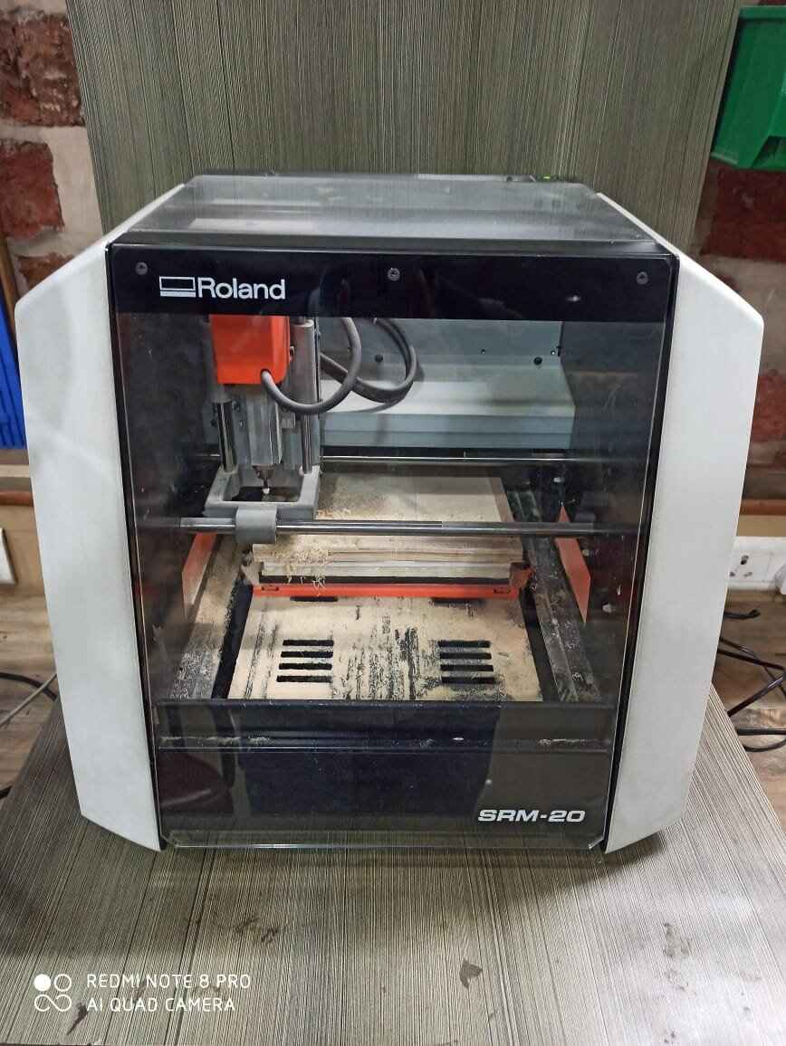
The SRM-20 portable milling machine can mill a broad range of materials, including modeling wax, chemical wood, foam, acrylic, poly acetate, ABS and PC board. The following items are just some of the prototypes and applications made possible:
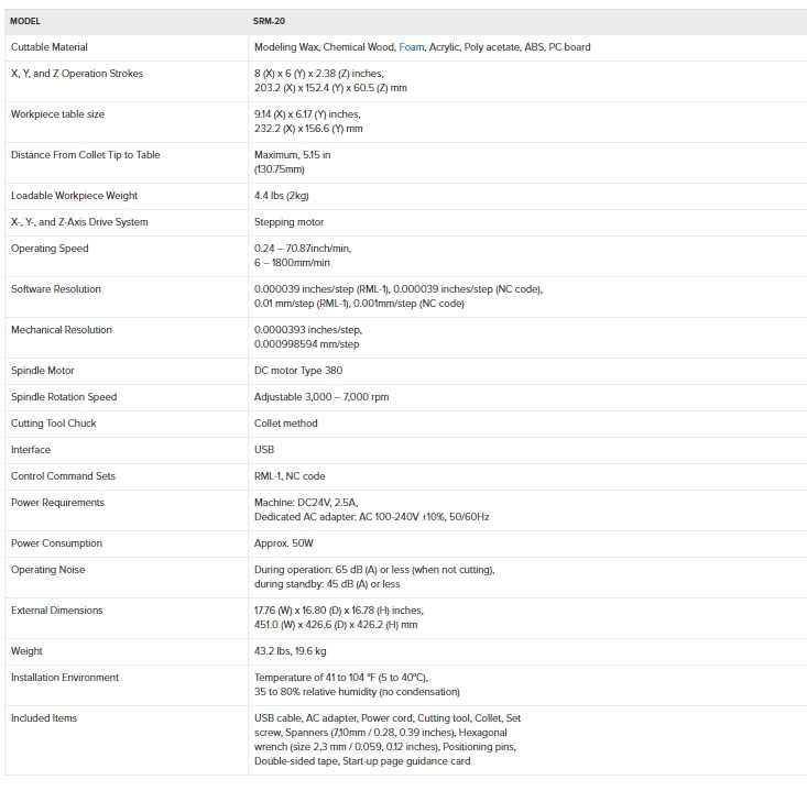
This is the basic Specification sheet of this machine if you want you can go through it
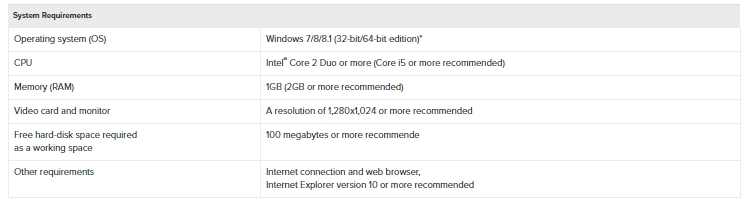
And these are basic system requirement to handle this machine
* If you more information about machine you can click on this link and it will guide you to a link from where you can know more about the machine
Software installation
Important note


                                          This installation should be done only in case , person decides want to control the machine by his/her laptop , otherwise its prefered that the user should use the existing system which is connected to the machine .

 Because in the case of bed leveling , the process can take several hours and it will not be easy to leave your system besides machine
STEP 1
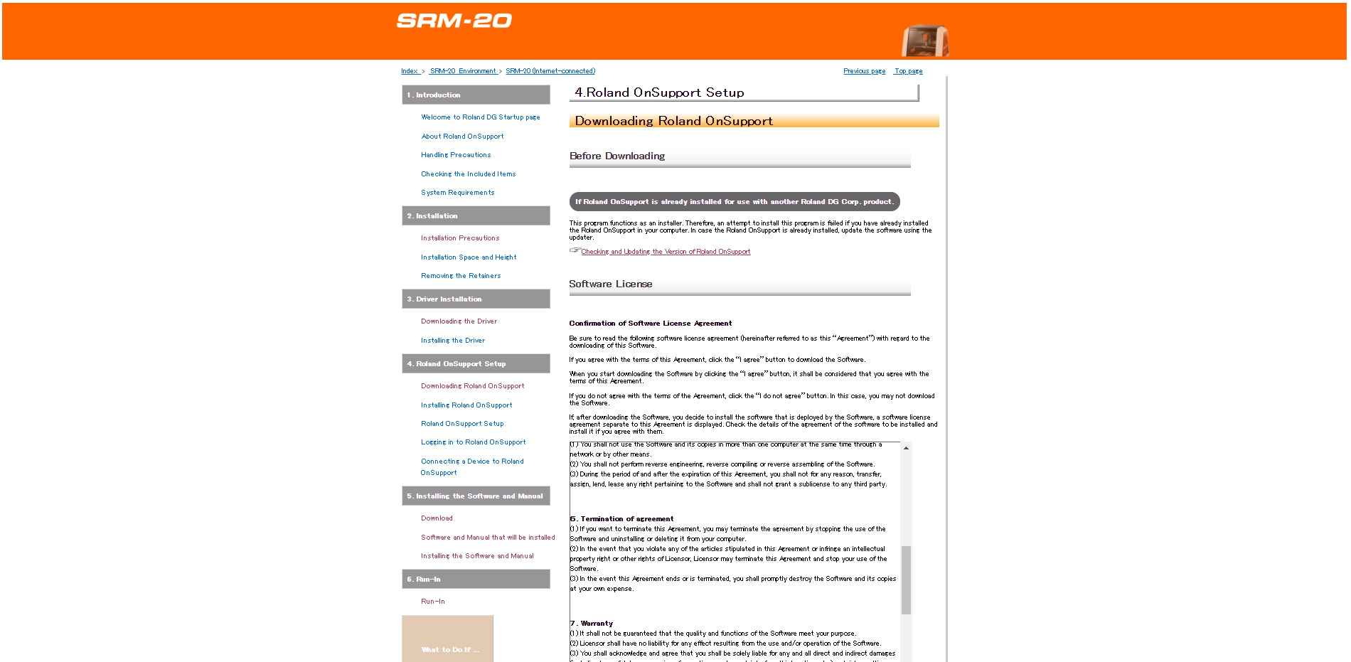
Go on thie website through this and download Roland Onsupport setup
STEP 2
After you installed the on support download its driver throught this
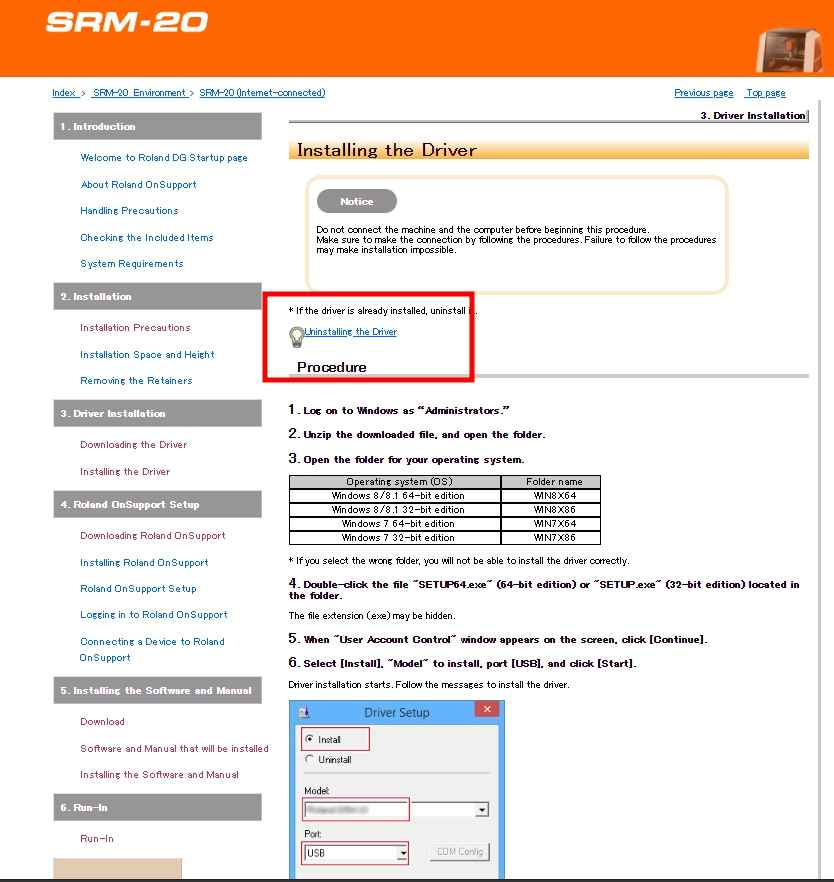
STEP 4
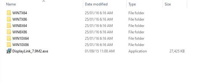
After downloading the driver's , extract them mand select the suitable driver which matches you computer configuration
STEP 5
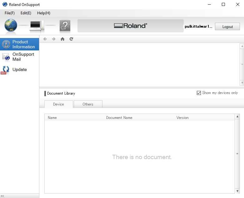
Once the driver is installed run the Roland Onsupport software which you previously installed.
STEP 6
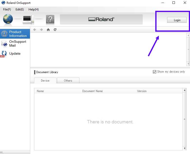
You have to make your new account and login through that to use the software.
STEP 7
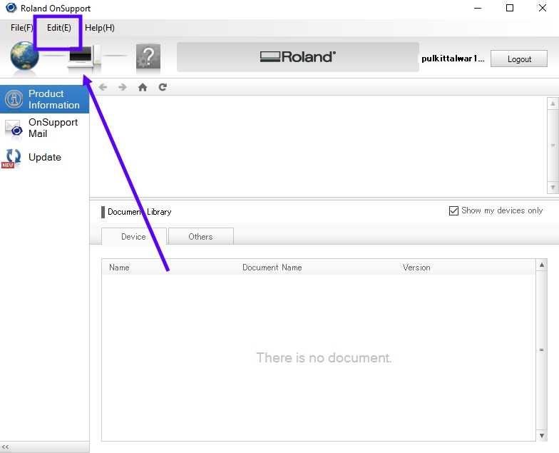
After login in go to the EDIT coomand on the top left section
STEP 8
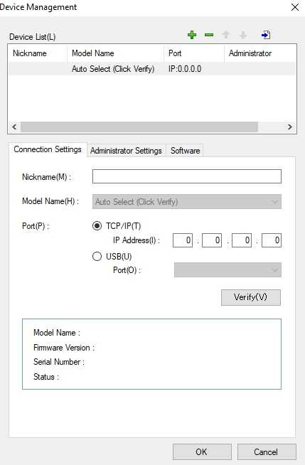
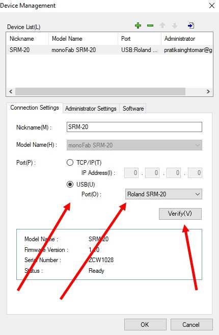
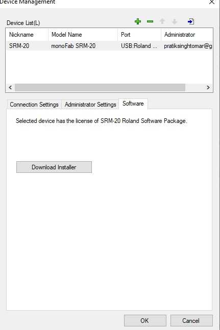
* Connect the machine USB to your system
Select
1. USB(U)
2. Ten the name of machine which you have
3. and then verify it
STEP 9
* And by clicking on software you can download the machine softwware
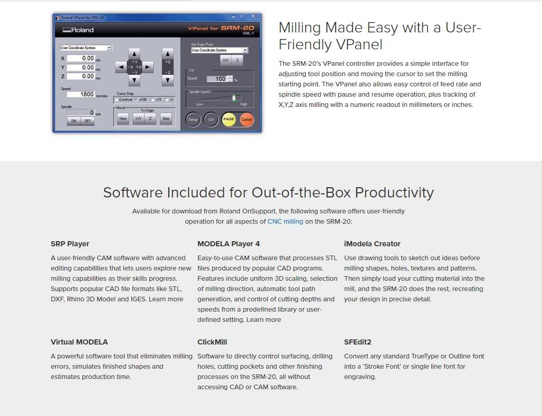
These are some basic software we can use
Material's required
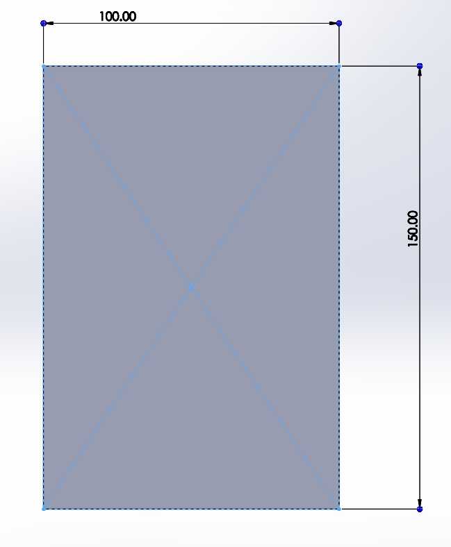
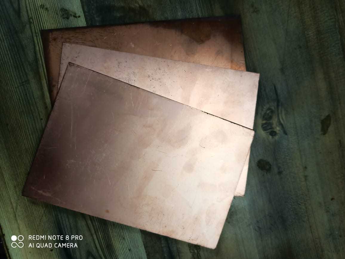
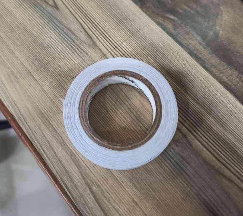
1. COPPER CLAD BOARD (150mm X 100mm X 1.5mm)
2. DOUBLE SIDE THIN TAPE
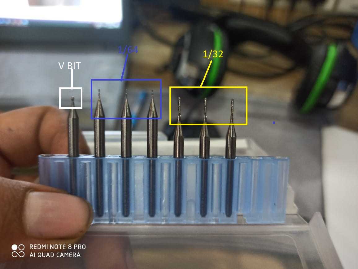
3. CARBIDE END MILL 3 mm
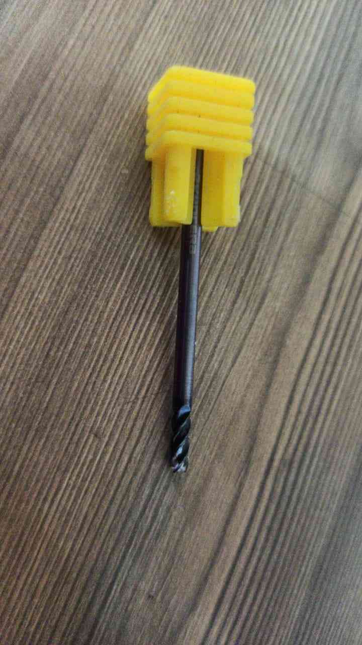
4. End mills ( 1/32inch, 1/64 inch, v bit)
PRE- PROCESSES
This is recommended to do these processes at before start working the machine
1. Before we start the assignment we need :
* Clean the machine
* Level the bed
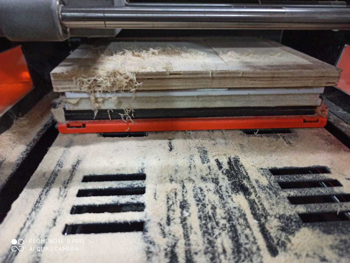
* After cutting a piece or using the machine always clean it for smooth working of machine
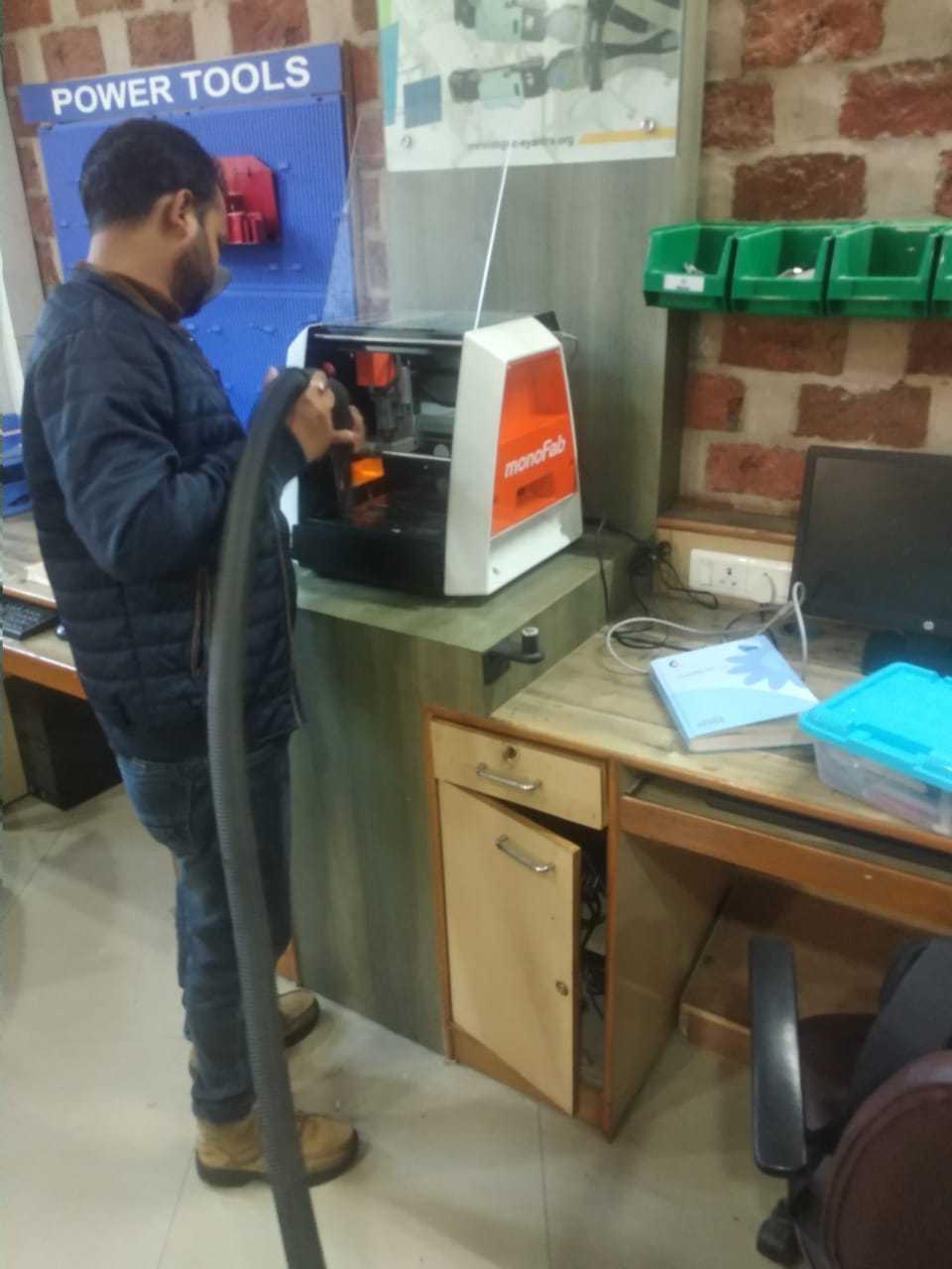
* Our local guru RAHUL GAUTUM is teaching us how to clean the machine using labs Vacum cleaner
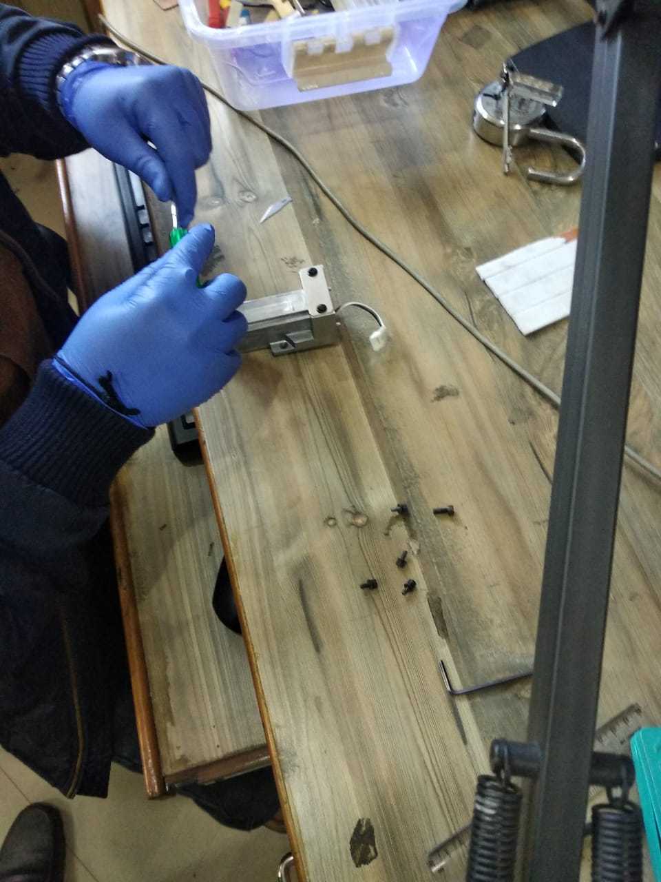
* Our machine is making too much noice during working so Rahul sir decided to overhaul the machine and open all the parts to give a detail cleaning touch
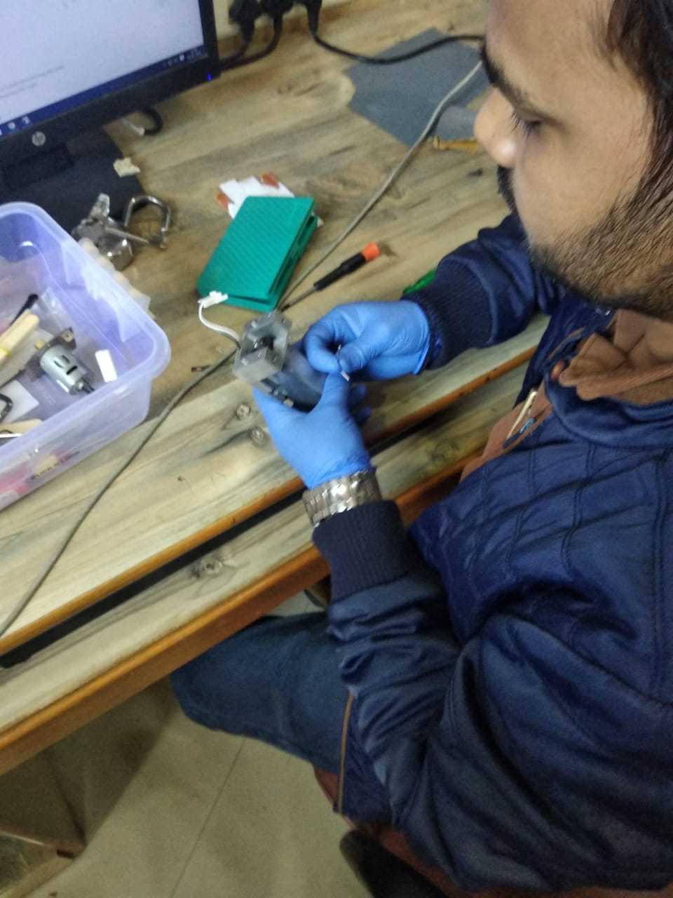
* Our machine is making too much noice during working so Rahul sir decided to overhaul the machine and open all the parts to give a detail cleaning touch
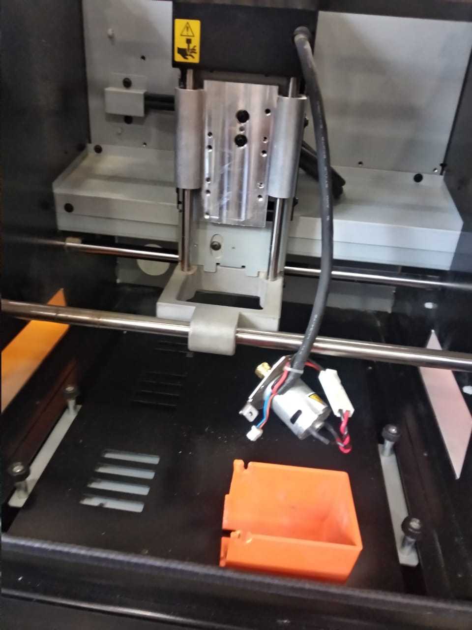
Right now the spindle and motor of the SRM are removed for service by our instructor,
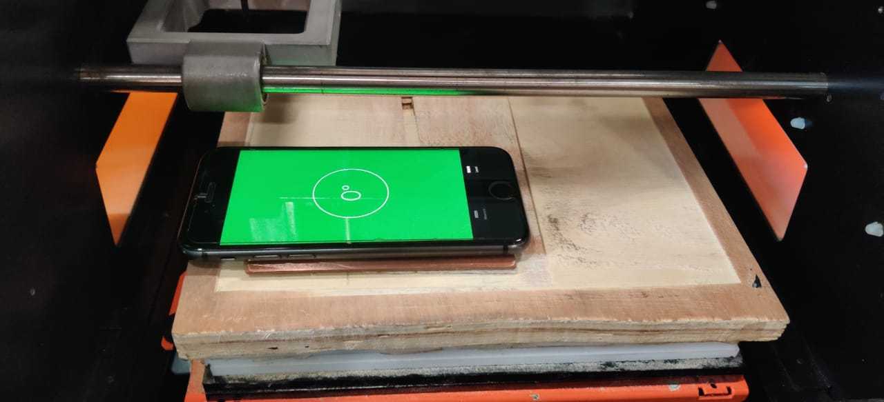
After cleaning we cleaned the machine we start to again level it, using a 3mm end mill
And for leveling you First this you need to download the CLICK MILL software from roland' s official site by clicking on this link
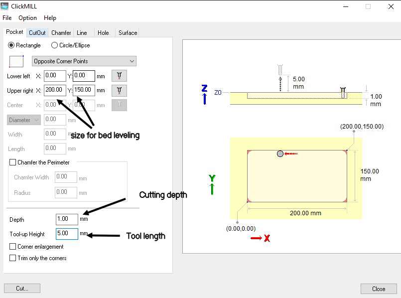
These are parameter i used for bed leveling
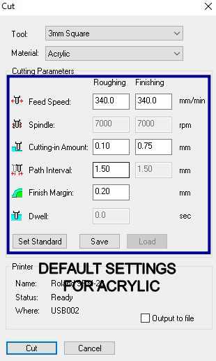
These are default settings for milling when you select the material they appears and in my advice let these be same as they are .
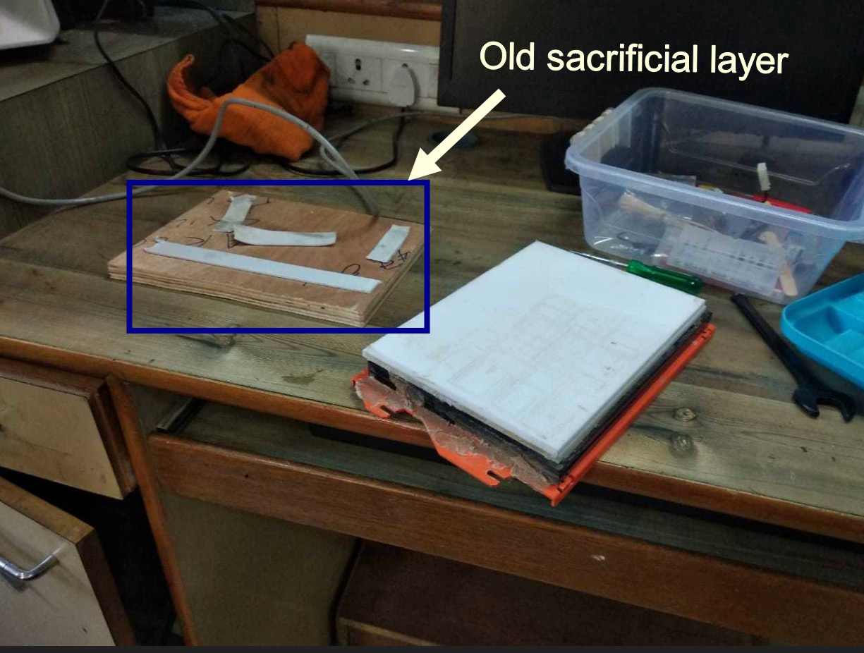
We saw that our old sacrificial layer wa not working well after 2-3 times of leveling , so our instructor removed that layer and thought to replace that layer with acrylic
He applied double side tape on the acrylic to replace the old layerto
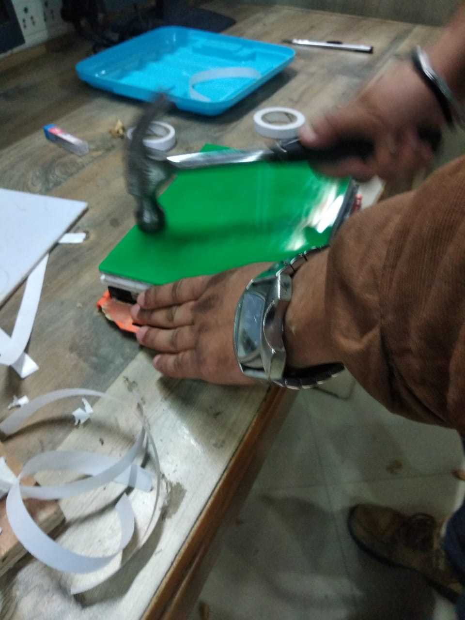
And hammered it firmly so that tape will properly stick on the acrylic
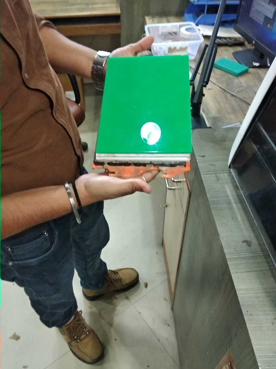
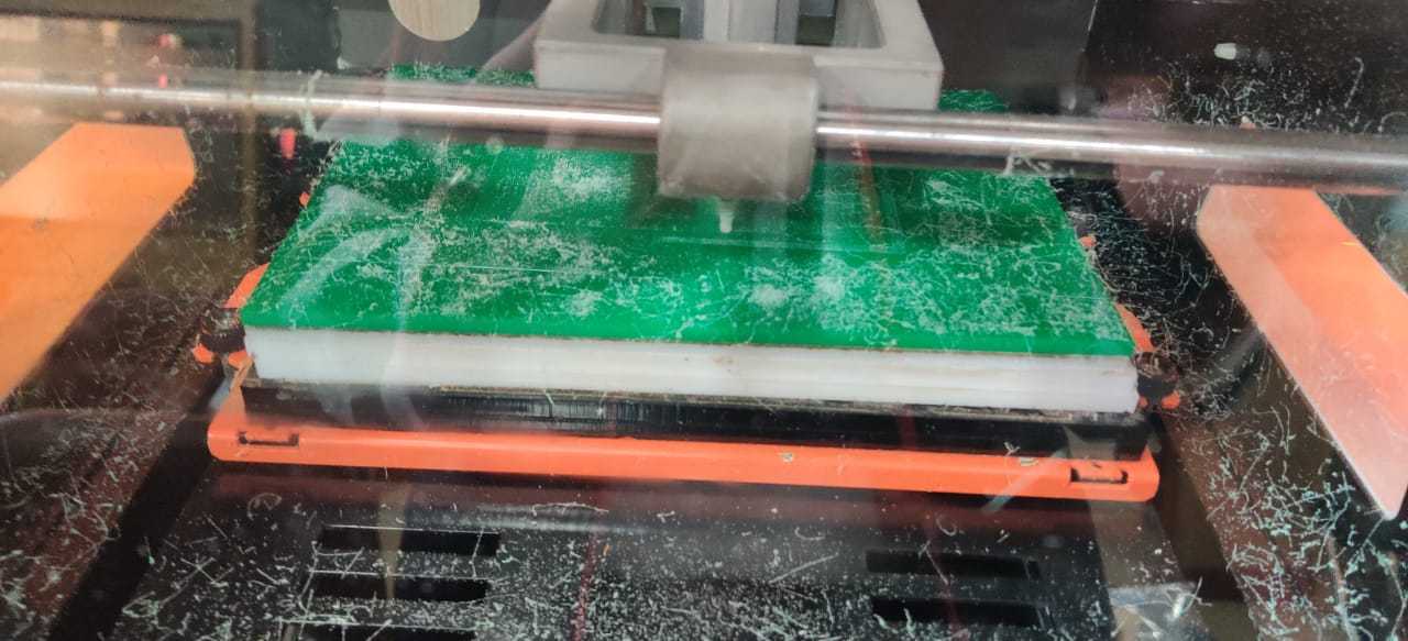
We again leveled the bed and this time it works
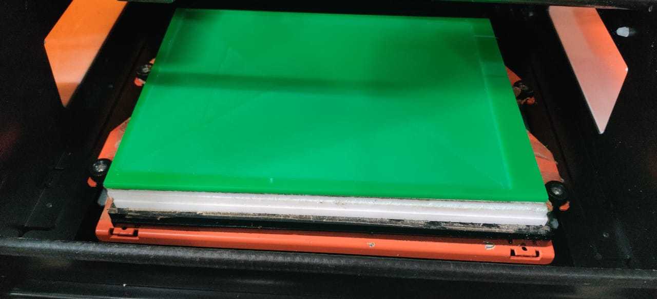
* after that we paste copper clad board on the leveled base and start cutting PCB
Cutting PCB
For designing a pcb we require a .rml file which we will use to create G-codes and M-codes For now we use the given png file and convert them into .rml file for cutting
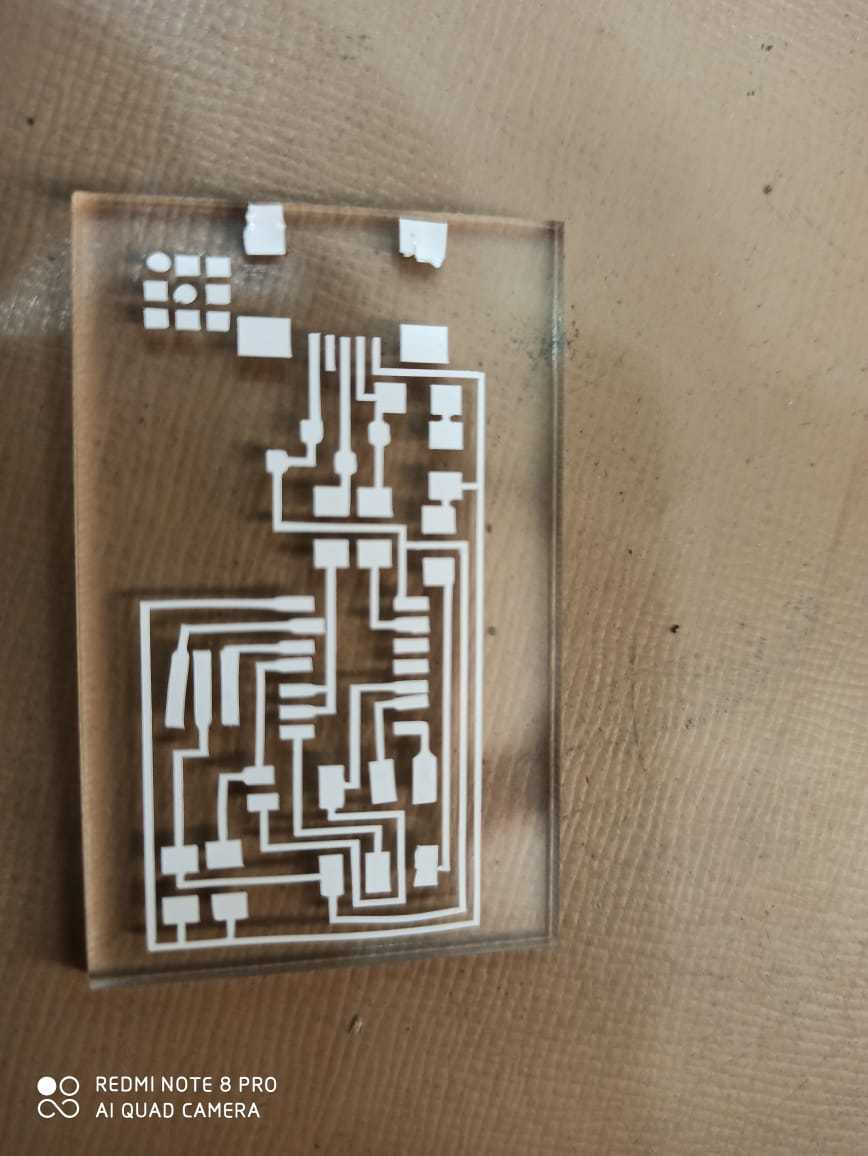
* This is image for png file which we have to use to check the accuracy of the machine.
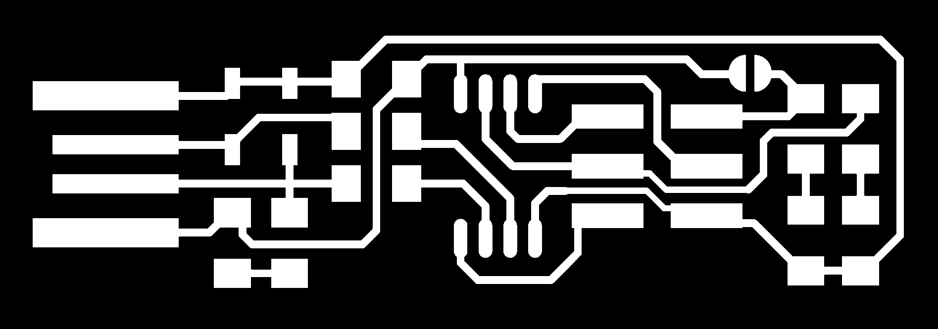
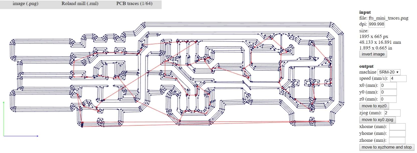
* This is the file which we need to mill and Solder the SMD (Surface mounted devices) components on it.

* This is the png file for outer bordering of "FAB ISP"
Images in png format can be downloaded using this .
Steps for converting an PNG image into .RML file
* After downloading the images , click on , to convert PNG file into .rml file
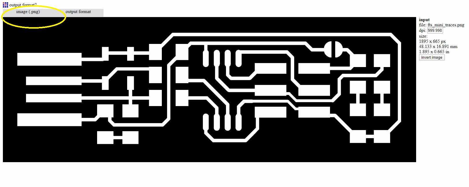
* Select which type format you are using for image.
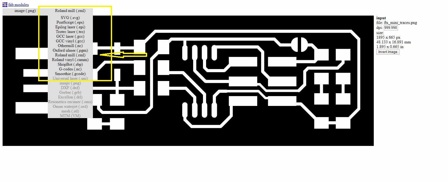
* Select the format in which you want to convert the file.
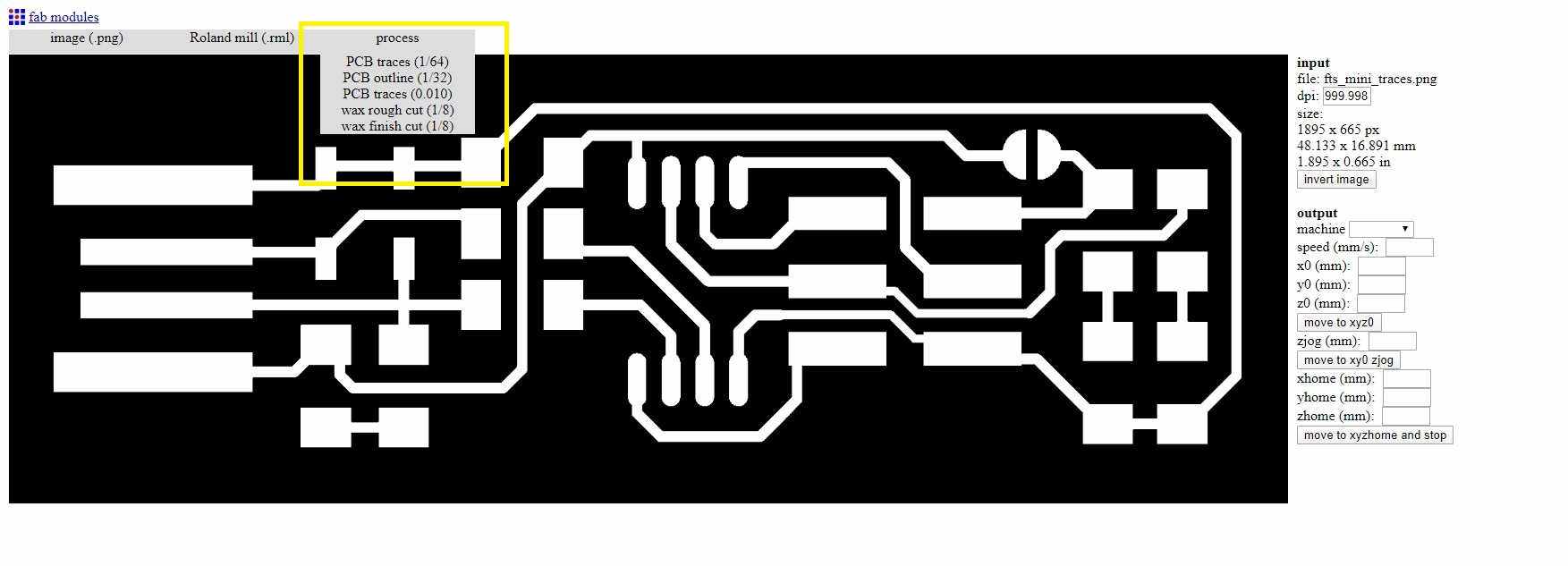
* Select which diameter of bit you want to use for operation.
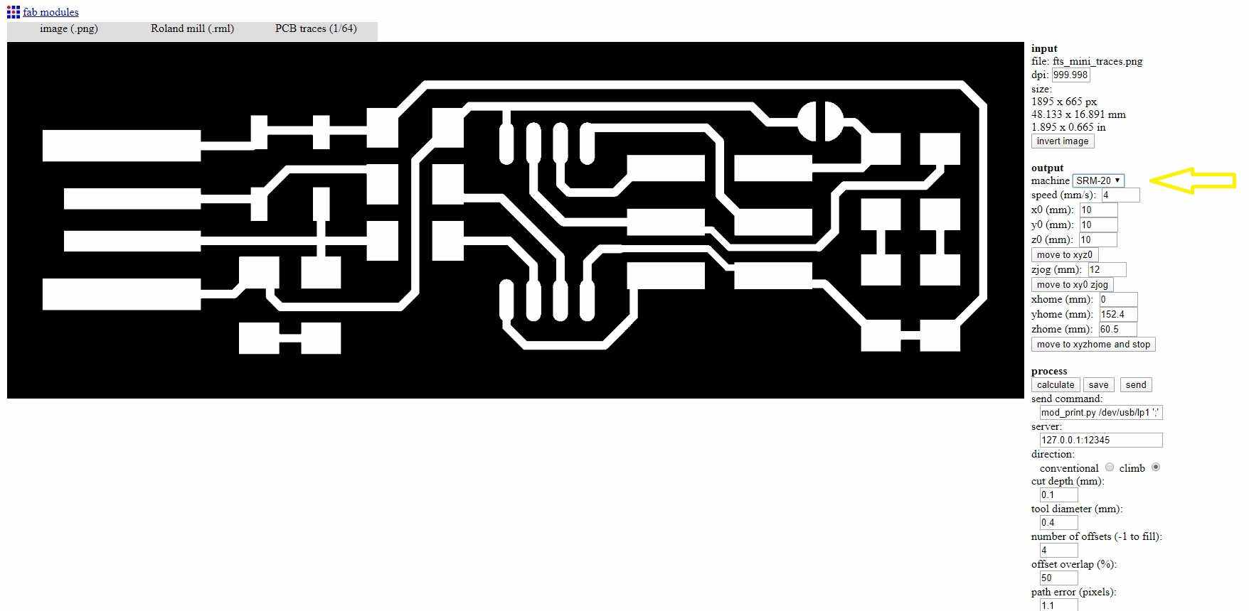
* Select the machine which is available in your lab.
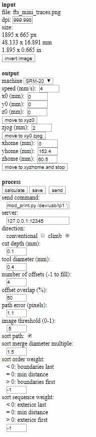
* Give 0 for all 3 axis and then click on calculate and then download the image.
* It has offset of 4 and this is the actual tool path which machine is going to take
I am providing .rml file here in case you want to use that
Fab ispSOME INFORMATION
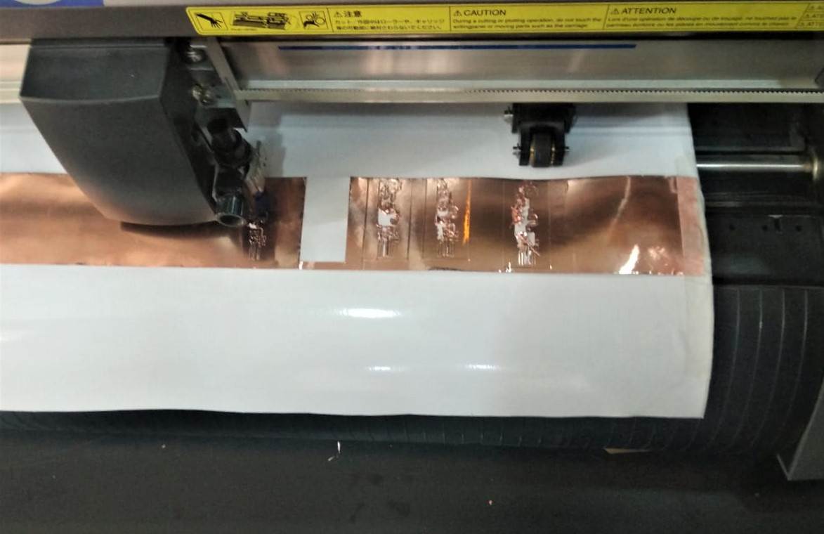
Due to 'COVID 19' virus logistic was hit and our lab was not able to procure some important supplies including clad board , Attiny controller , milling bits and many more things which effected workflow of this week , so alternatively we have to cut pcb on vinyl cutter and its documentation is as follow.
* First we cutted 'FAB ISP' on white vinyl sheet using our labs vinyl cutter and based it on trasnparent acrylic disk which we cutted on the laser cutter
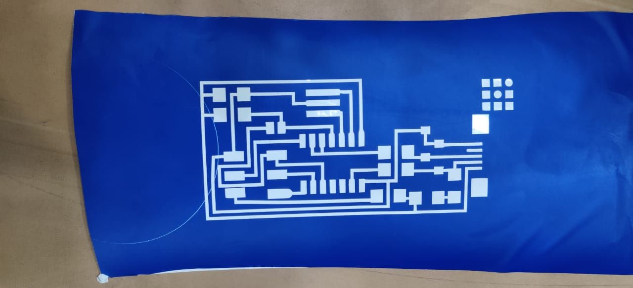
* Secondly we cutted brian's board using same method which I previously stated
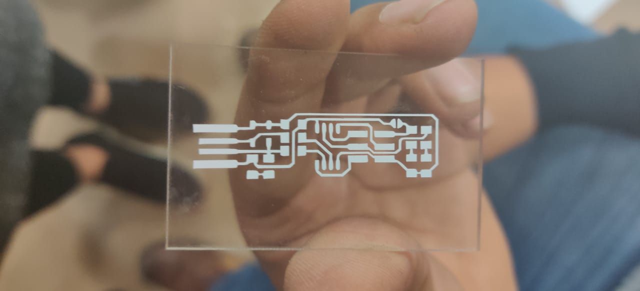
Flexible copper PCB
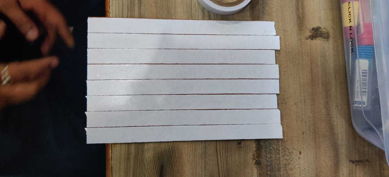
* Then we try to make a flexible PCB on copper tape using same method , but it was a big failure , because of very thin film of copper which tends to cut by optimizing parameters but when we try to paste it on the
acrylic disc it never worked
* and in this process we almost waste whole copper tape in optimizing the best parameter , but it was a failure.
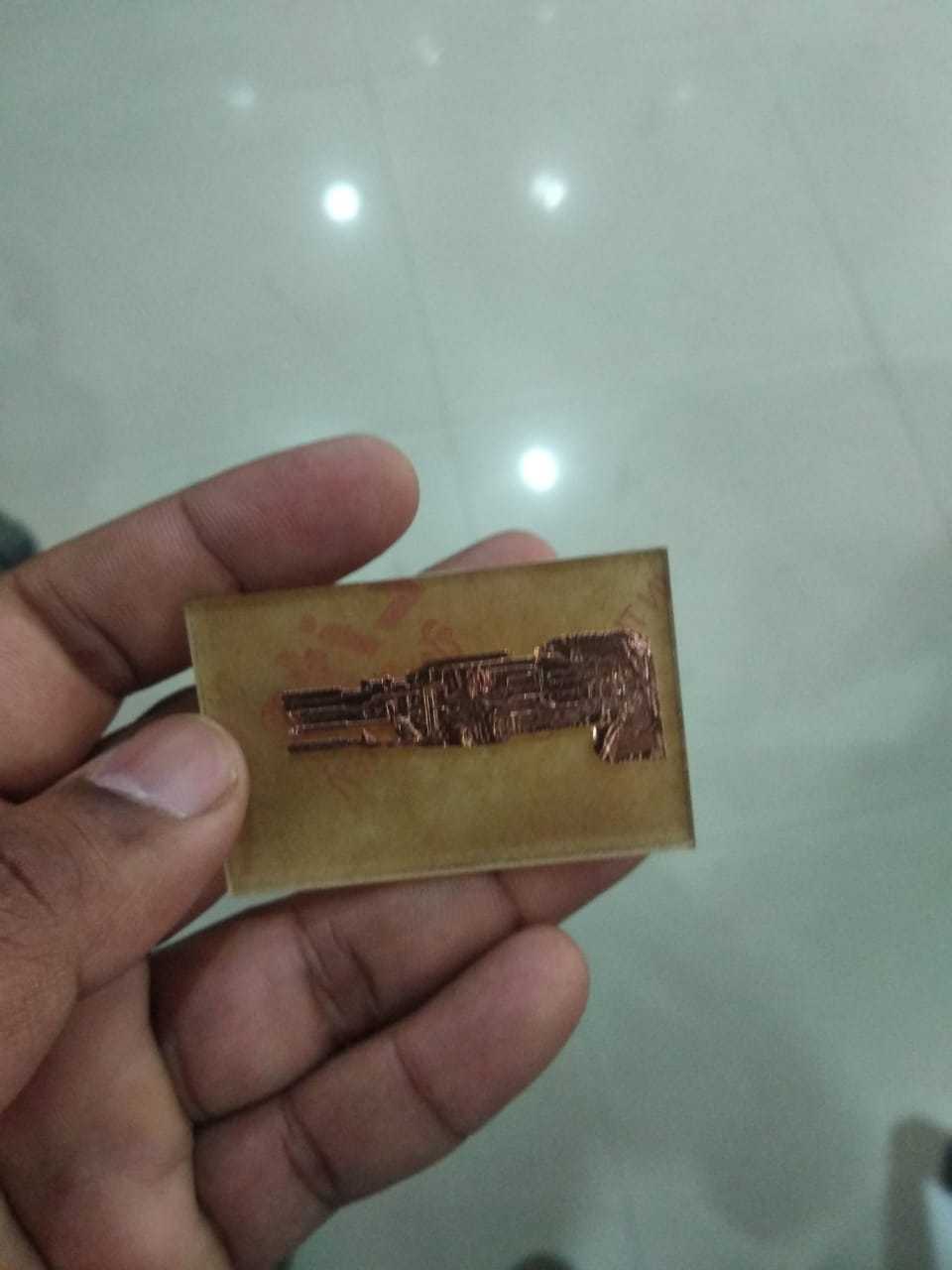
* You can see thhe above image , it is one of the best try we have and it was stil not upto the mark.
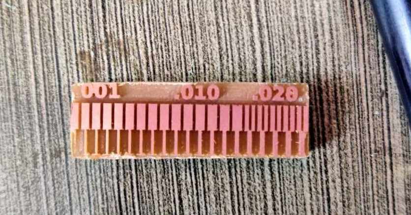
GROUP ASSIGNMENT
*For group assignment we need to characterize design rule for PCB , and you can download the design through this
and its outer outline through
TEST FILE
ITS OUTLINE

* In this case the depth of cut was too much so unfortunately it cutted too deep almost upto the base layer.
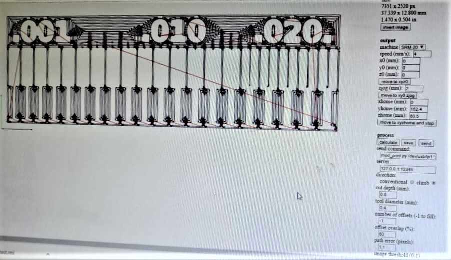
TEST 1
Tracing parameter
* Tool used = 1/64 inch end mill
* Tool Dia = 0.39 mm
* Depth of Cut = 0.8 mm
* Offet = -1
* Offset Overlap = 50%
Cutting parameter
* For cut we used 1/32 inch end mill
* offset = 1
* Depth of cut = 0.4 mm
* Stock = 1.7mm
* Tool Dia = 0.89 mm
* As you can see it has too much depth because initially we gave 0.8mm, so we planned to try it again with less depth.
TEST 2
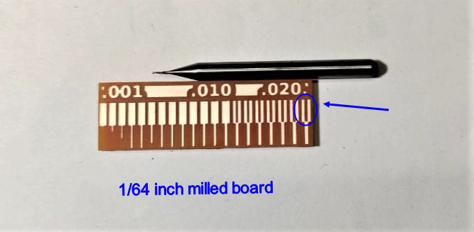
Tracing parameter
* Tool used = 1/64 inch end mill
* Tool Dia = 0.39 mm
* Depth of Cut = 0.1 mm
* Offet = -1
* Offset Overlap = 50%
Cutting parameter
* For cut we used 1/32 inch end mill
* offset = 1
* Depth of cut = 0.4 mm
* Stock = 1.7mm
* Tool Dia = 0.89 mm
This is much better as we reduced the depth of cut and got great results
TEST 3
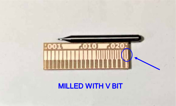
Tracing parameter
* Tool used = V-Bit
* Tool Dia = 0.35 mm
* Depth of Cut = 0.12 mm
* Offet = -1
* Offset Overlap = 50%
Cutting parameter
* For cut we used 1/32 inch end mill
* offset = 1
* Depth of cut = 0.4 mm
* Stock = 1.7mm
* Tool Dia = 0.89 mm
* As you can see in these image the cuts are not smooth and this lacks a little bit of finish , but yes v bit can also be use for this purpose. it gives quite good results.
CONCLUSION
1. We find 0.1mm depth of cut appropriate for traces.
2. The maximum clearnace come out to be 0.013 inches or 14 mil
3. The Trace width cuts uptto 0.006 inches or 8 mil.
I am providing .rml file here in case you want to use that
Test cut file
* We were asked to individually convert png image into .rml file and mill the board ass well as solder the respective components it.
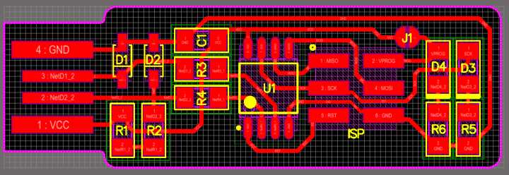
* You can get an exact idea how you should place parts on the the PCB. through this schematic
Now its time to cut hte pcb , ready your .rml file which you made previously for pcb
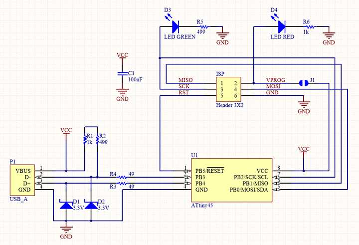
* All the comprehensive details regarding the board is given on this you can go and also view it.
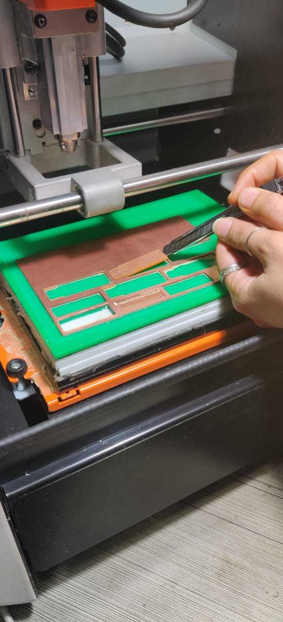
Steps for soldering components on the copper board
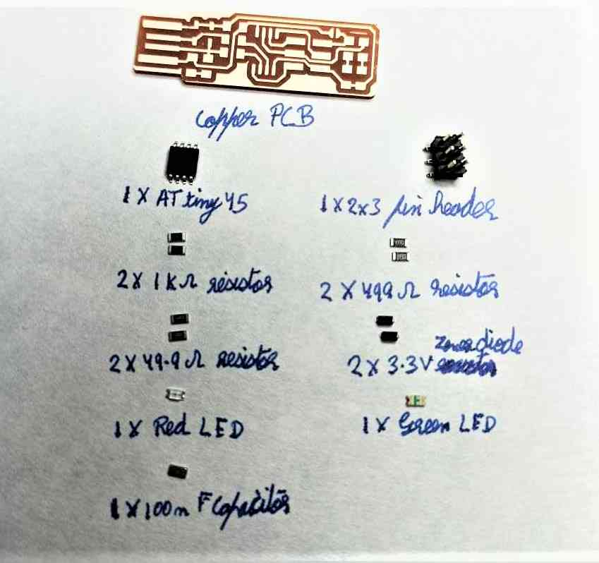
* Pls collect these components before starting soldering.
PLS WATCH THIS VIDEO BEFORE STARTING SOLDERING YOUR BOARD
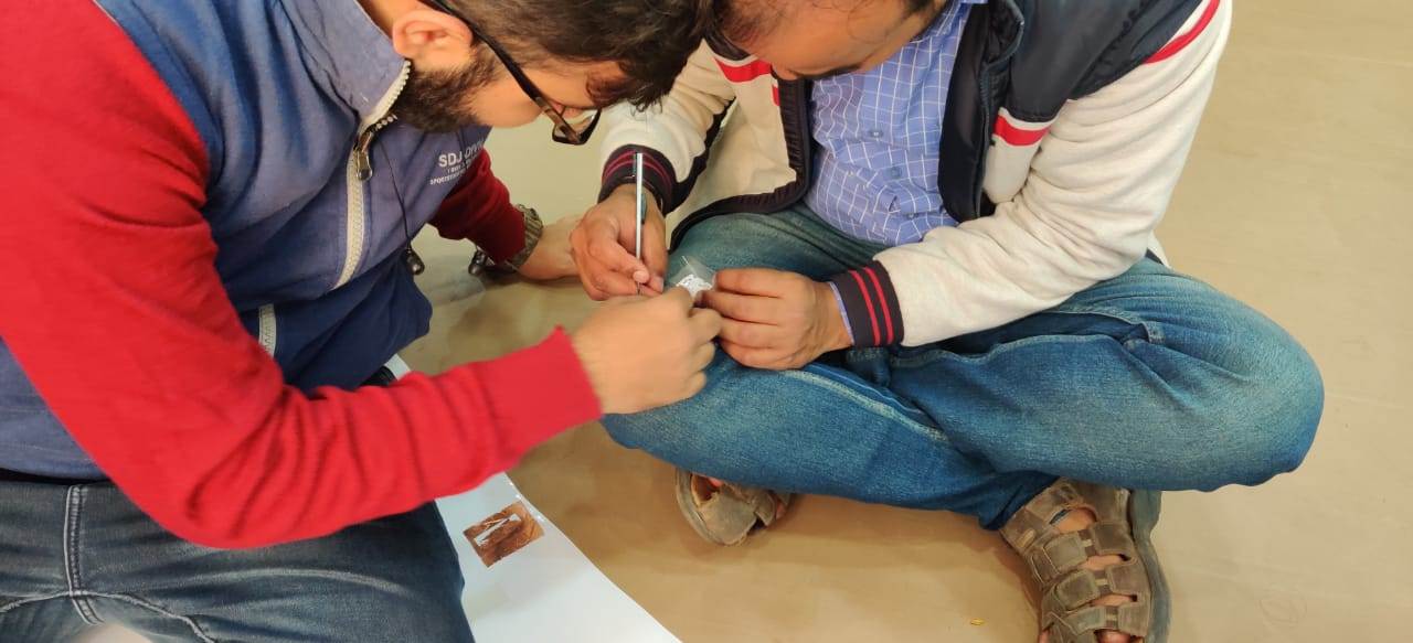
This soldering process was performed by our Local Guru RAHUL sir , and he is teaching us how to solder the PCB
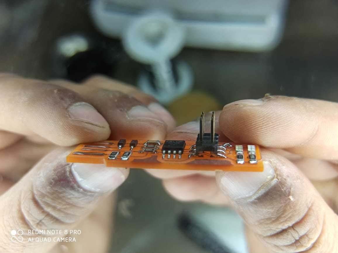
* This is a perfect example of exellent soldering
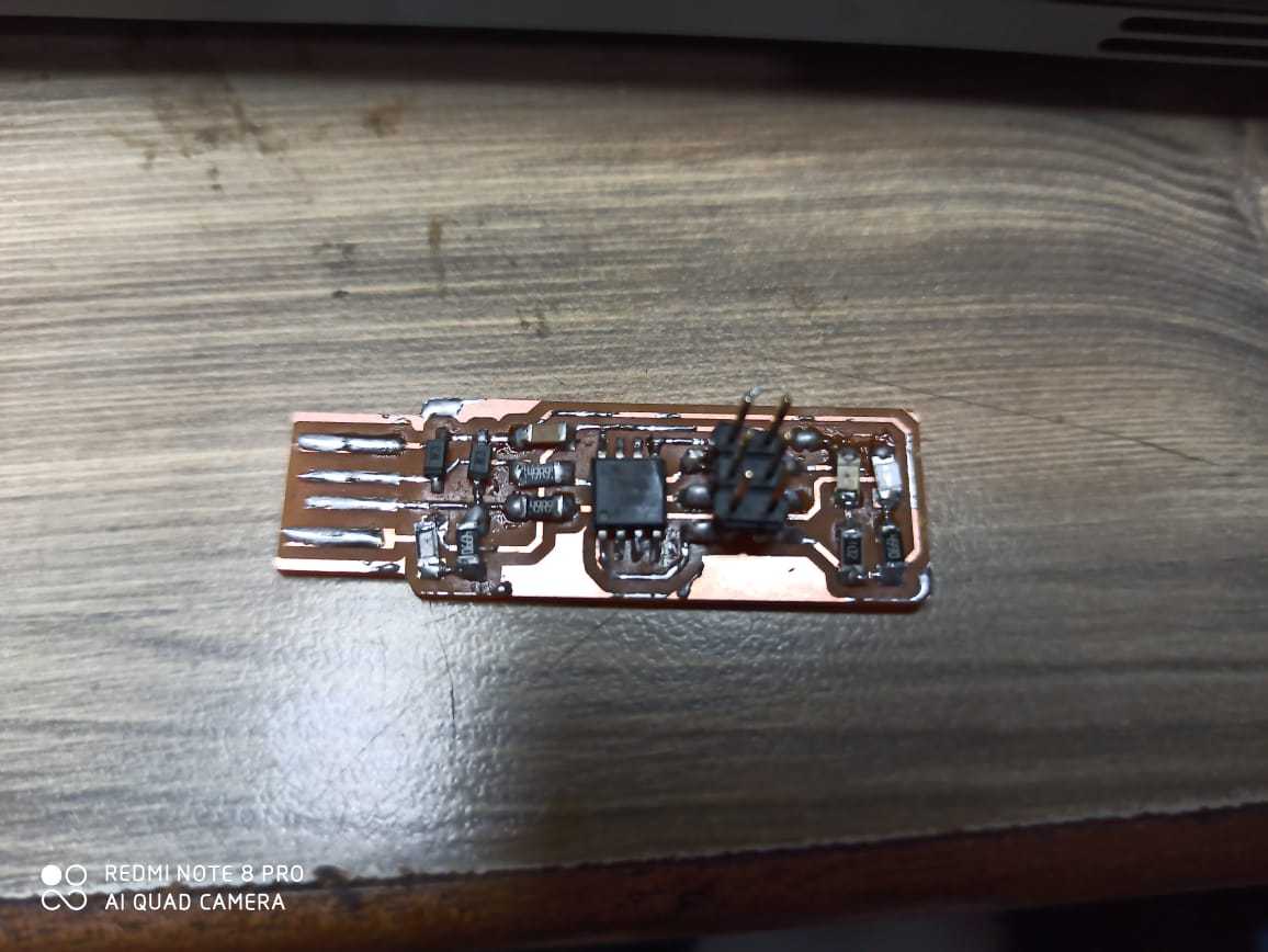
And this is the example that how you should not solder PCB i.e my PCB
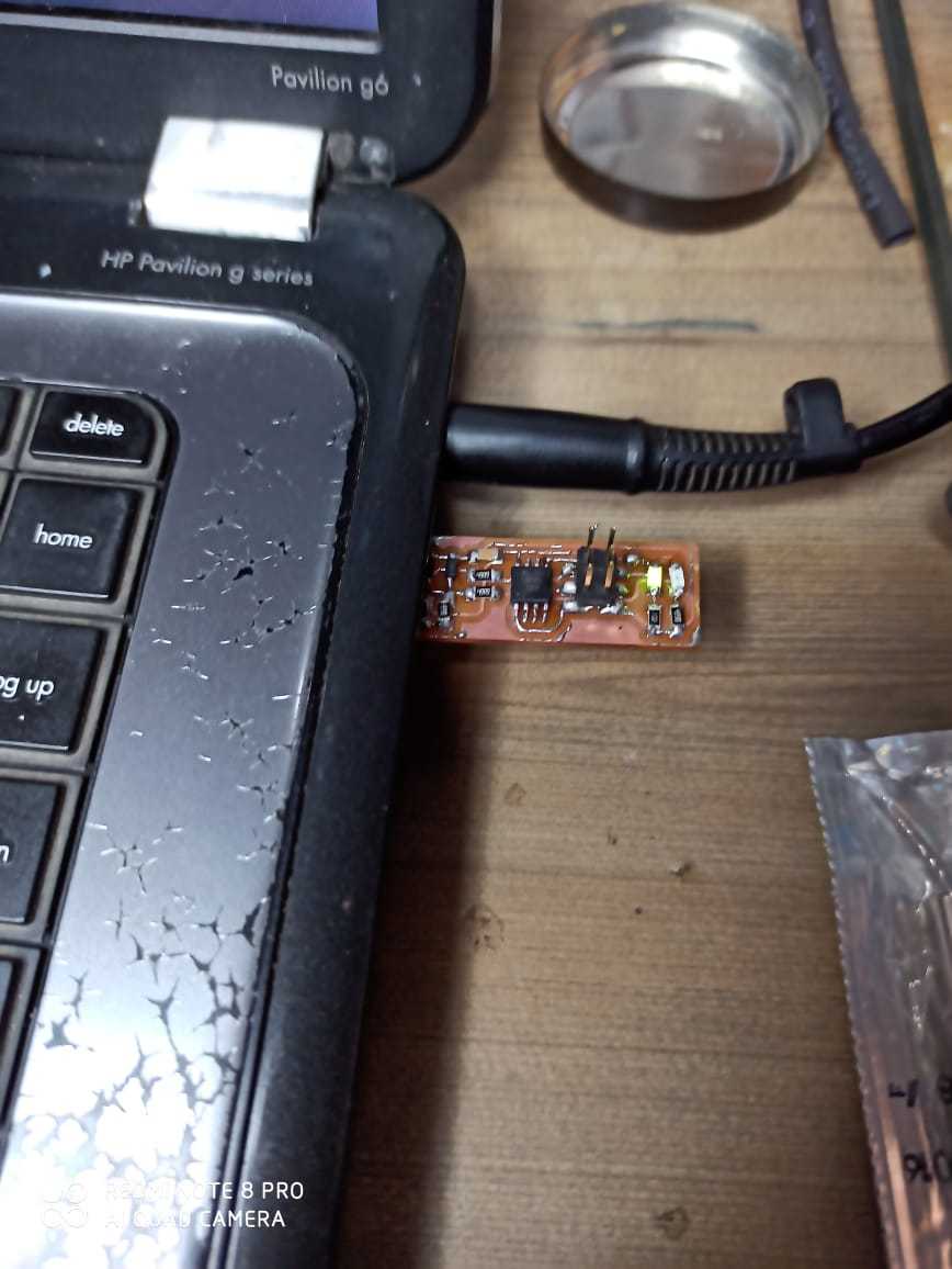
* But fortunately it works and the moment i connected this in my system , my system recognize it .
Programming of PCB
Now we have program the PCB so that it is able to progam other PCBs. . so for that purpose you need to download these
1. Atmel GNU Toolchain2. GNU make
3. AVRDUDE
4. Zadig
5. FTS firmware
Software installation
There are some steps which you require to perform during downlaoding of software and ii have mention those here
1. Atmel GNU Toolchain
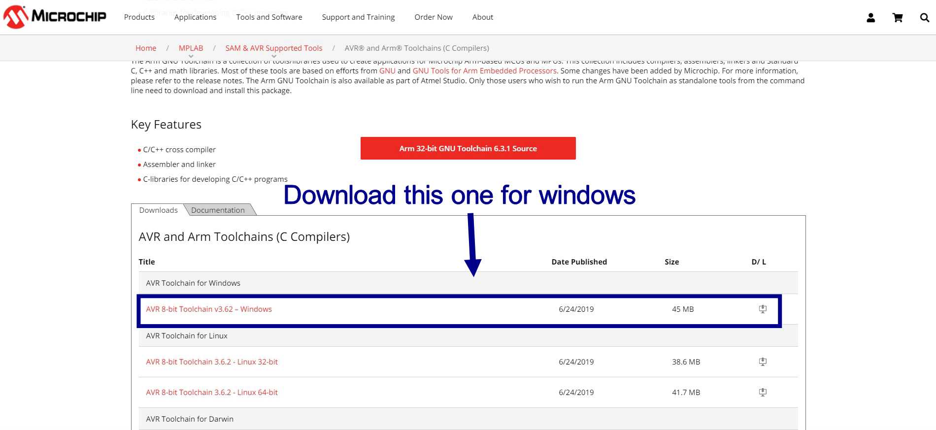
After clicking on the link you will be guided to microhip official page where you need to perform some steps
For downloading software you required to make an account and it is a lengthy process
After the GNU TOOLCHAIN is downloaded you can easily download other software , but please zedig for now
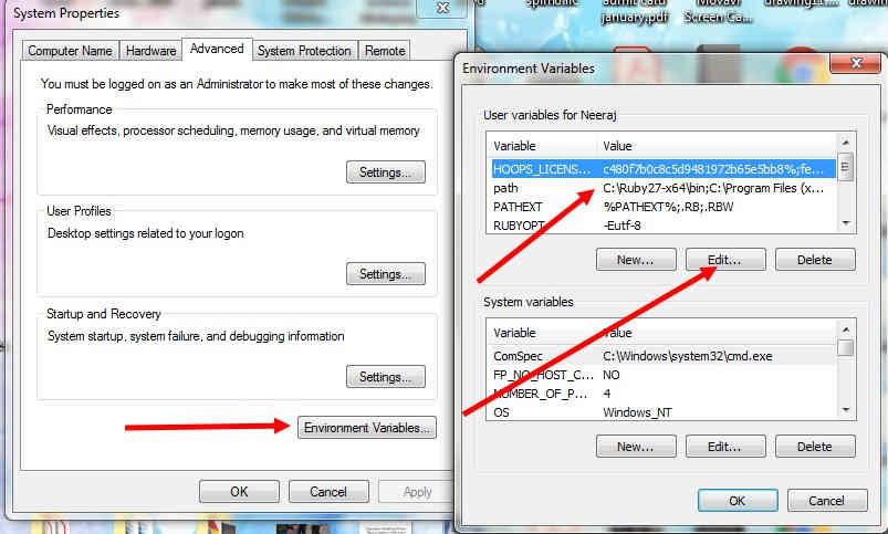
you need to add paths of GNU toolchain, GNU make and AVRDUDE by going to the control panel >> system and security >> system >> advanced system settings >> environment variable >> double click on paths >> and add the new paths.(Please refer to this image).
After you did this step install zadig
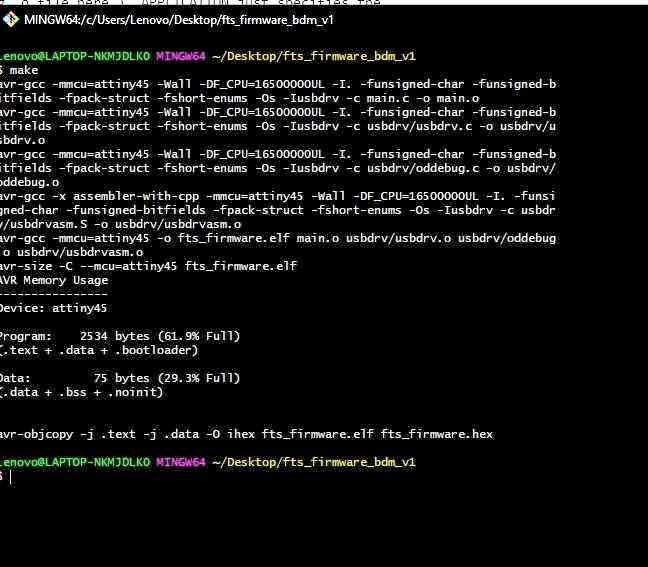
Right click on the firmware directory and select git bash, and enter command MAKE to create a hex file
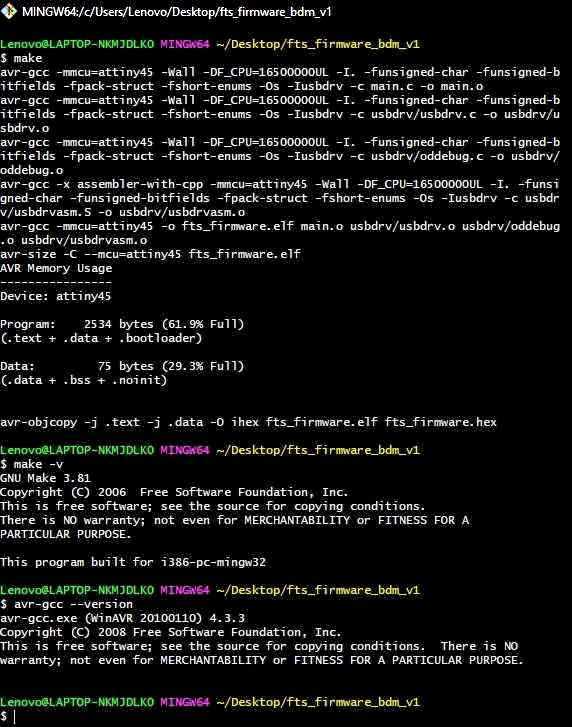
Once the hex file is generated you need to add these commands to check wheather the right make software is installed MAKE -V and AVR-GCC --VERSION
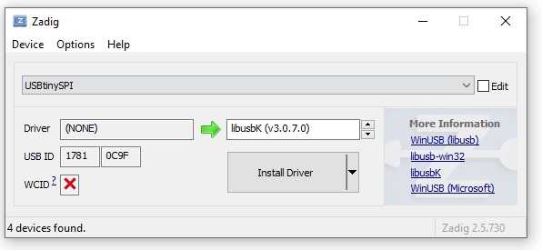
Connect your AVRISPMKII to your Computer system and open zadig software
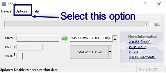
When you open the software you will see there are no boards showing there then you need to click on OPTIONS >> LIST ALL DEVICES and it will show all the available boards, but you wont able too see AVRISPMKII there so
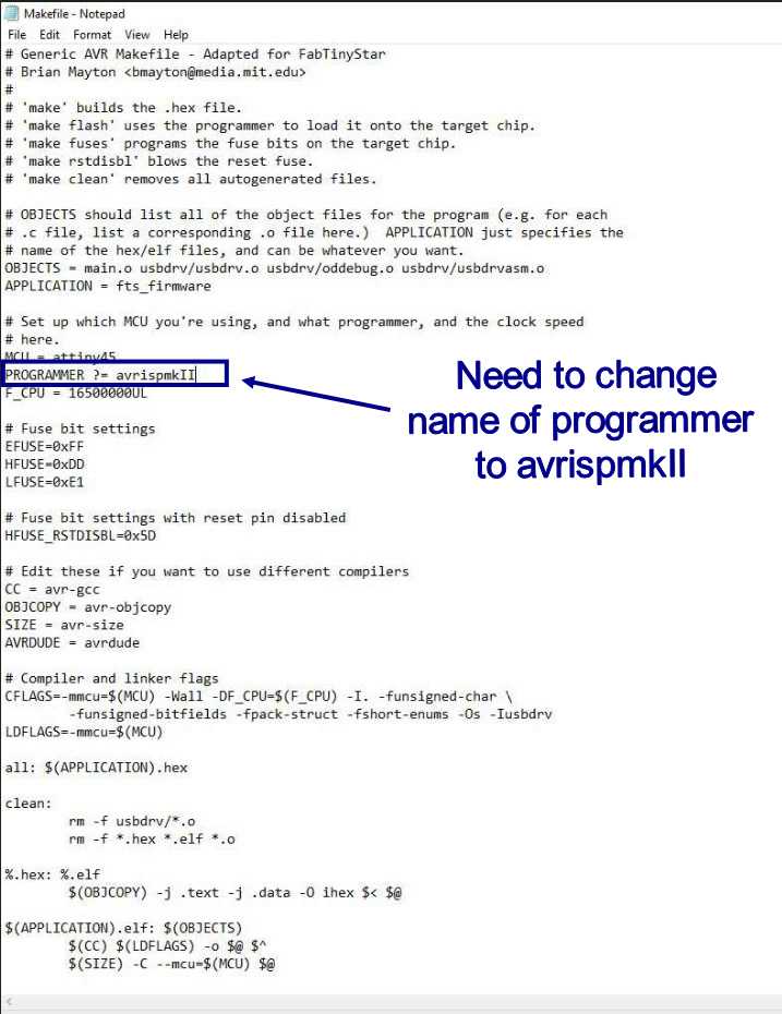
For system to see your programmer you are required to do some changes in the make file in firmware repository , you need to change the name of programmer to AVRISPMKII from USBTINYISP , once you do this zadig will recognise the AVR programmer
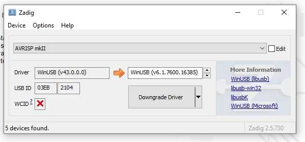
You can see the programmer is visible
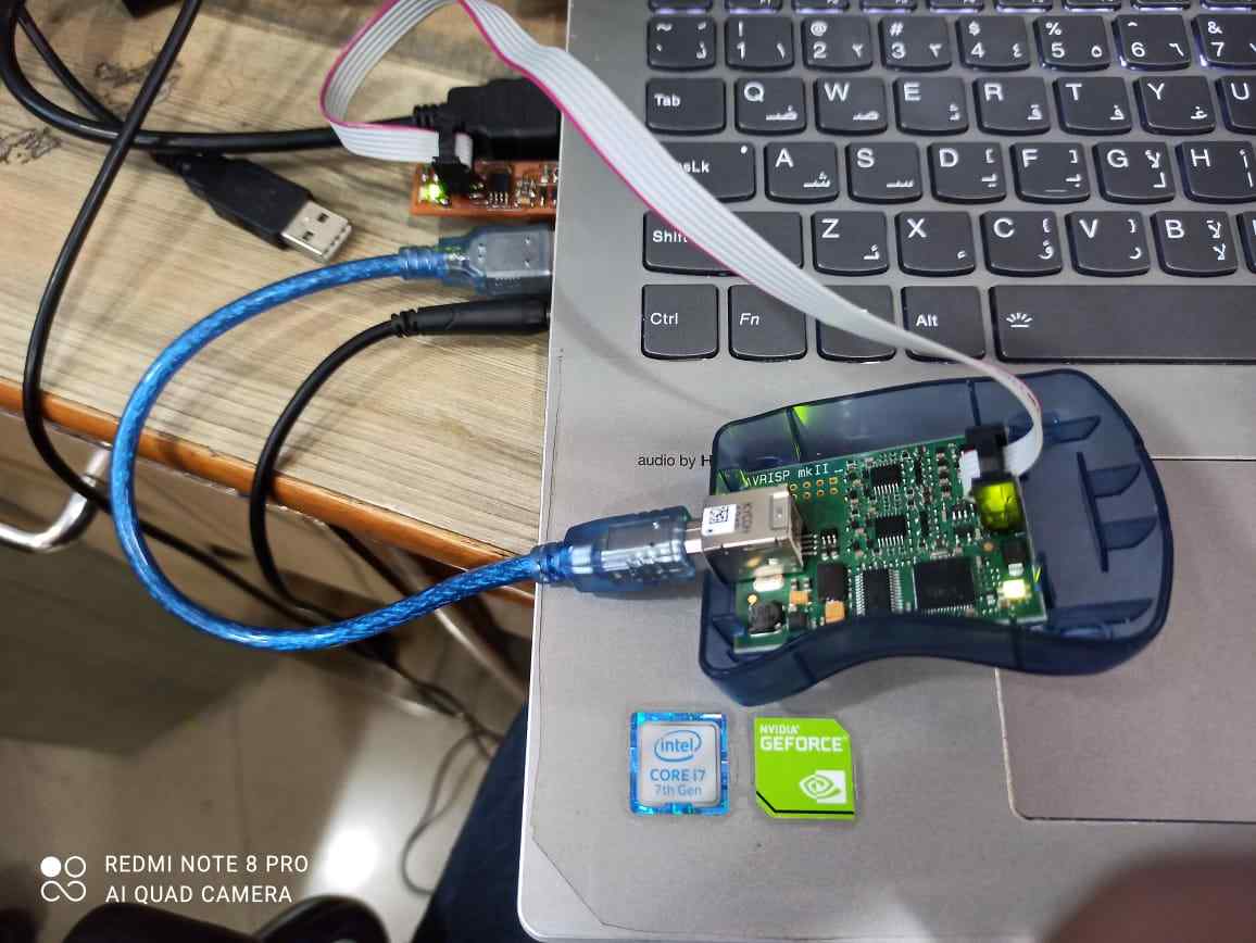
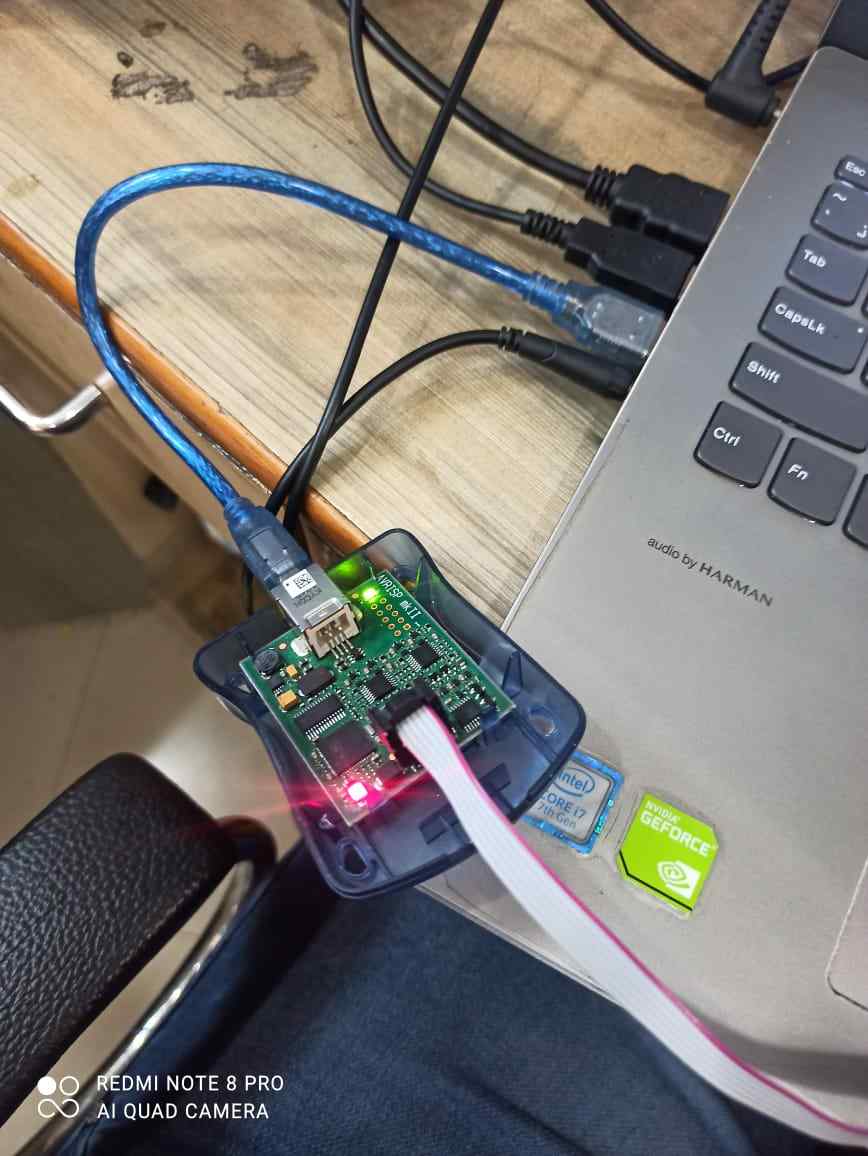
Now you need to connect the FABtiny isp you made with you system as well as avr programer like what i shown in image , so you can program it now
When you connect he pcb there can be 2 possibilities ,
1. You have connected the connectorin apposite direction
2. you connected that right
to know that you have connectedcbcorrectly please look to the videos i have given below
If pcb is connected wrongly then the led starts blinking rapidly and you will know that you have connected it incorrectly so just rotate the connector
And if connected the connector correctly then there will be no blinking light
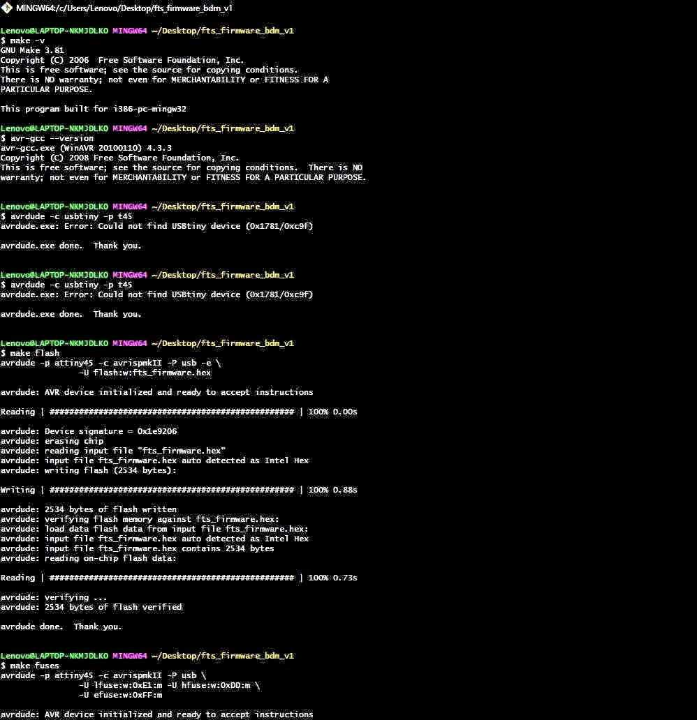
Then comeback to the GIT bash and give these commands MAKE FLASH
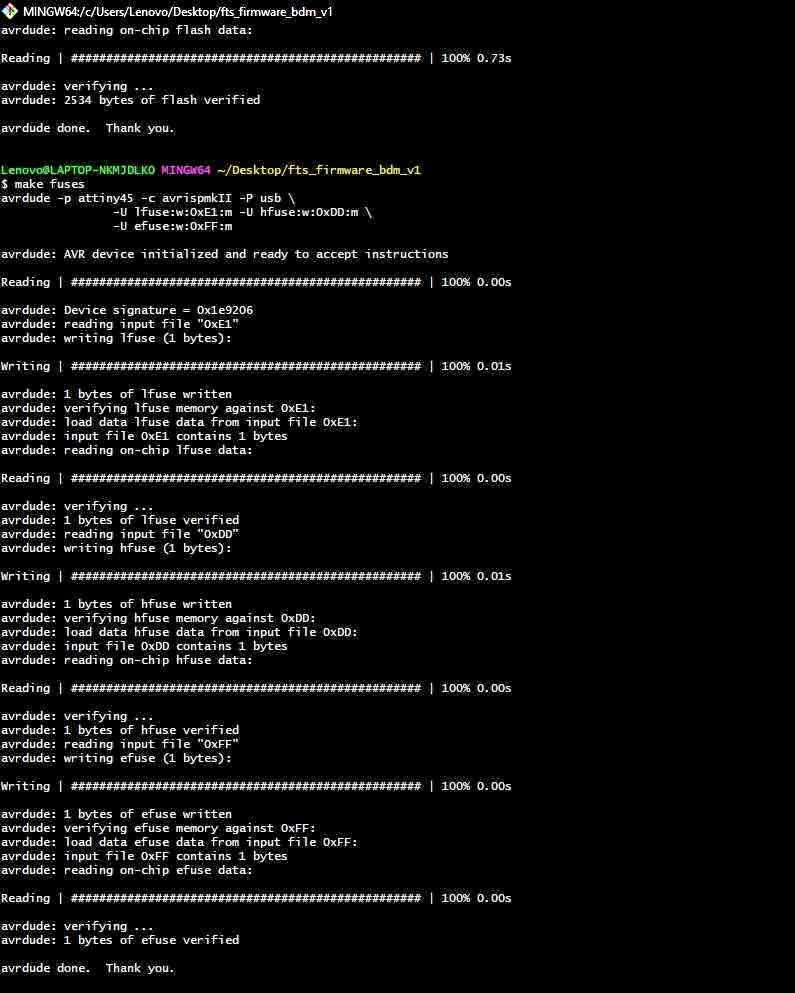
Then this command MAKR FUSE now your pcb is programmed
Now you require to install drivers and then open zadig and click on the install drivers
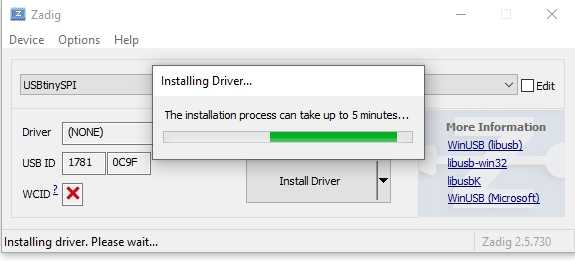
It will take a little bit of time to install drivers so please wait for sometime
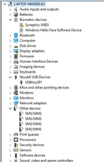
Then to check wheather every thing worked or not open device manager anthere you can see the usbtinyisp
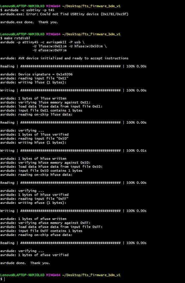
The last step of programming the ISP is to reset fuse by giving the command make rstdisbl.
This command will disable the ability to re-program the board in the future by changing the reset pin of the board to a general purpose input output pin.
If you like to know how to use FAB TINY ISP as a programmer pls click on this link , there i have programmed a board as well as shown how you can also program a boaerd by yourself