Tenth assignment
20 February 2019
Week's assingment
This week's assignment consists on redrawing the echo hello-world board, add a button and LED check the design rules, make it, and test it.
Echo Hello world board
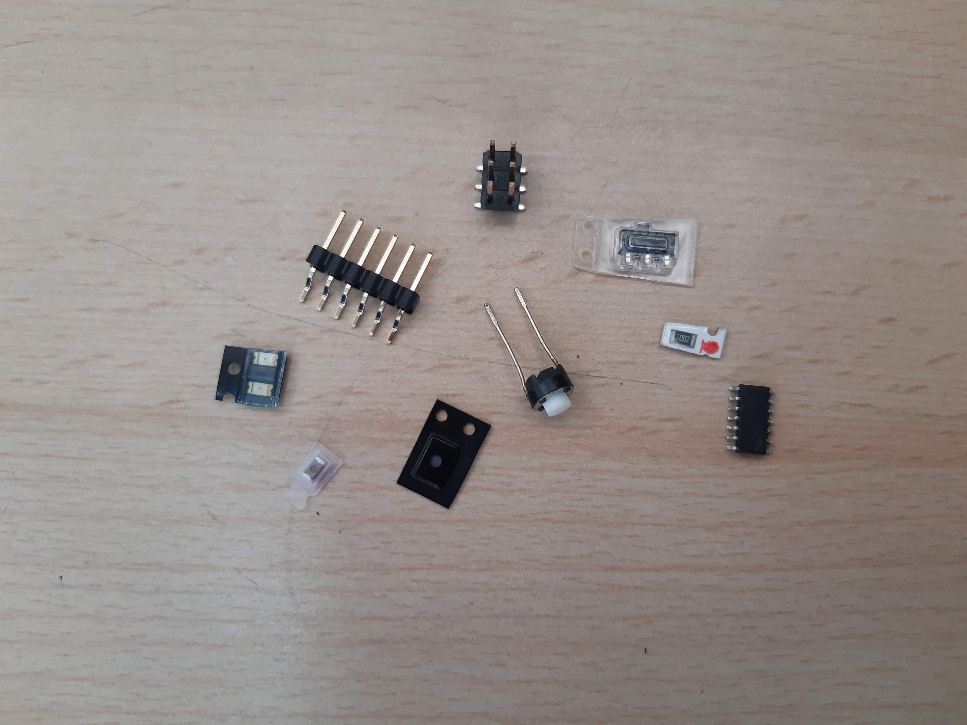
Components
I am absolutely a newbie in this field and until actually making my own board it all looked like an undecipherable code for me.
First step should be to know what are we making, what will it do, and what will we need to fabricate it and make it work.
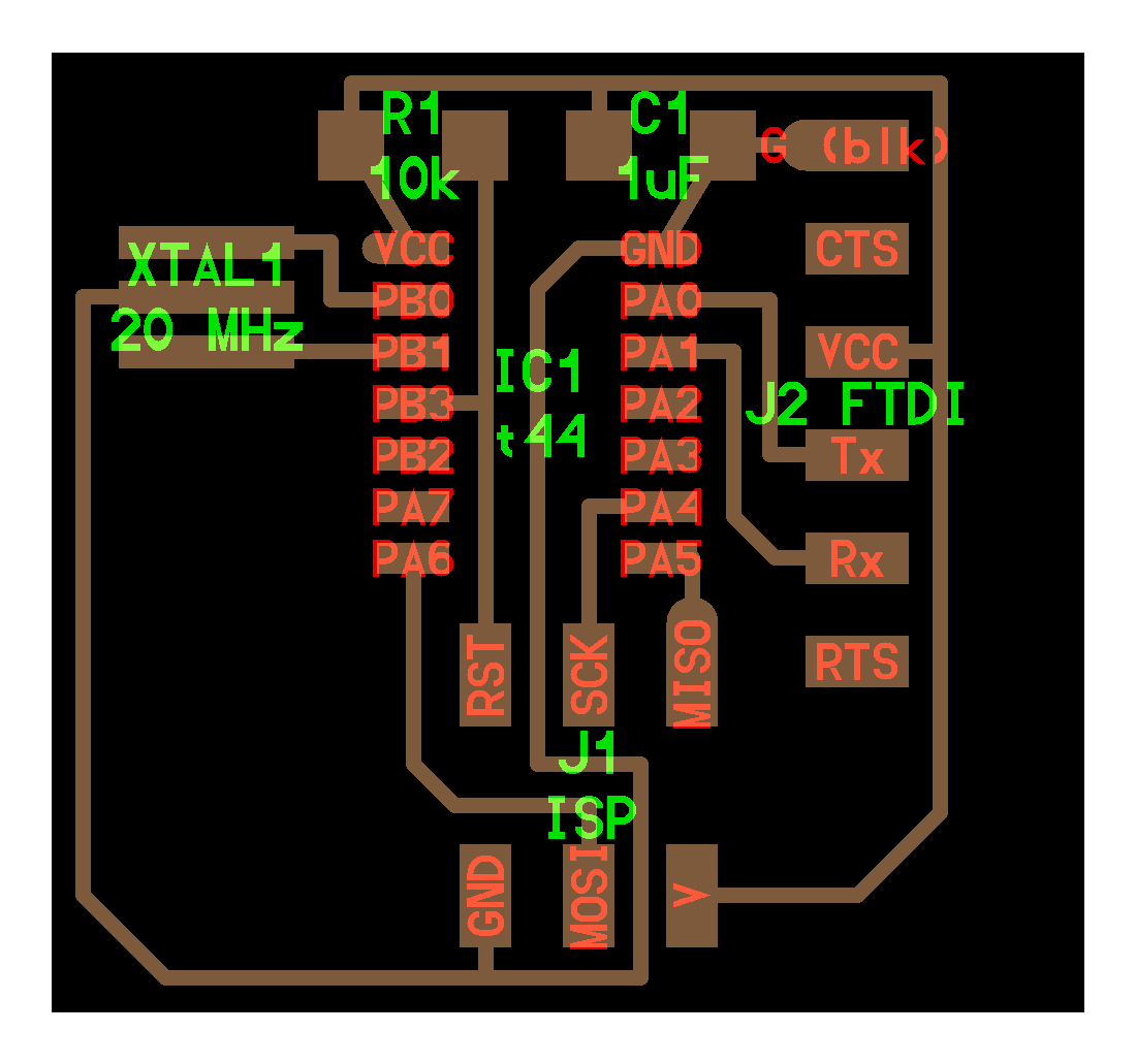
First thing I did was making a list with the electronics I needed, following the image above, and asked the person in charge of the components to lend me those.
list
Attiny 45 microcontroller
10k Resistor (2)
1uF Capacitor
ISP pin header (2x3)
FTDI pin header
LED smd
499 ohm resistor
LDR
The basic function of the resistor is to reduce current flow, adjust signals levels and divide voltages. To calculate it's value you can apply the Ohm's law. R=V/I, V being the voltage drop across the LED and I being the current. You can use an online calculator if needed. I applied 5V (for the attiny), 60mA and a 3.3 drop voltage. I got 28.333 Ohm, this is the minimum resistor's value I need for the green smd LED that I am using. For this assignment it is suggested to use a 499Ohm resistor (which I am going to be using), this is a higher value and the only thing that will happen here is that the brightness will dim down.
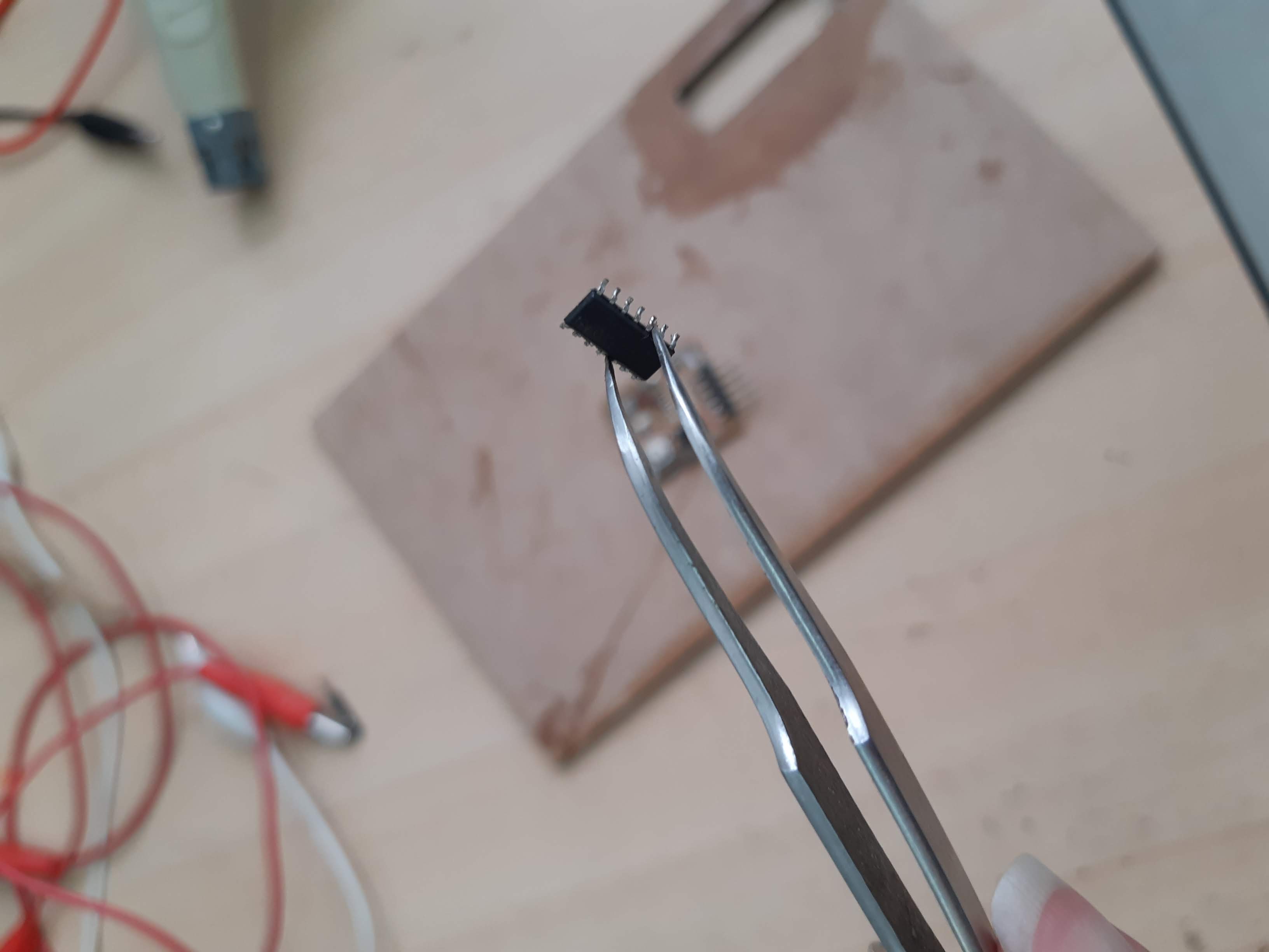
It turned out there were no Attiny 44 available, I had to steal one from a last year's student board.
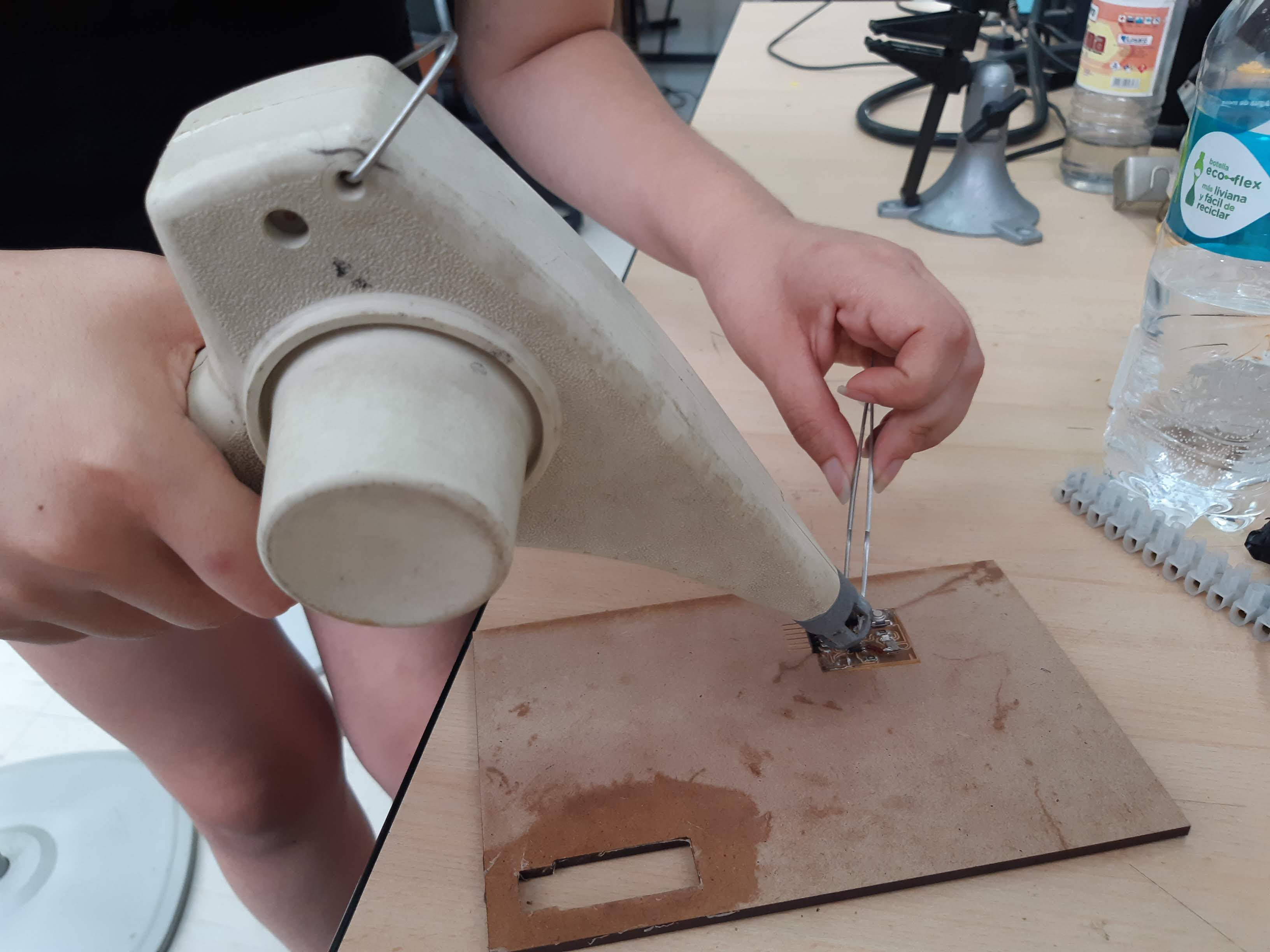
If you need to do this sometime, hold the Attiny44 with some tweezers and heat the board with hot air. It doesn't work immediately, just be patient.
I got almost all the components, unfortunately I got confused between the resonator and the crystal and I ended up with a quartz crystal smd (I actually realized about this later in my process, you will see if you keep reading).
Also there were not buttons left, instead I got a slide switch and later I got a two pin push button.
Designing the PCB
Schematic
Before actually making the board and soldering the components we need to make an schematic drawing. We will put all the connections between the components there, and use it as a guide to establish all the routes without forgetting any.
For this part we can choose a PCB design software. I tried Eagle and EasyEDA but finally chose eagle for this part. It is a program from Autodesk that you can also download for free.
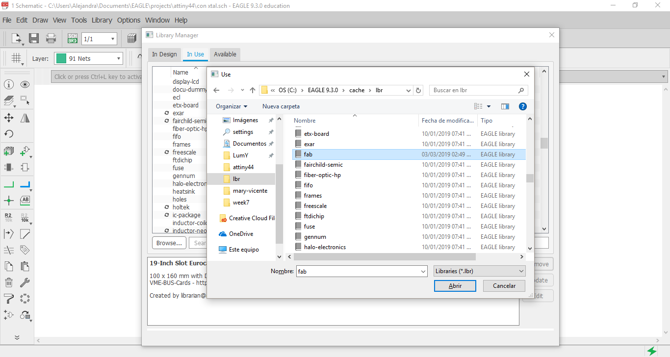
If you are going to use this program too, you may want to download and install the fab lab library, this is actually the reason I chose Eagle. You can find the archive fab.lbr here (you can download the whole file).
placing components
Once I had the library installed, I started placing all the components I needed. I just write the command "add" and look for what I needed.
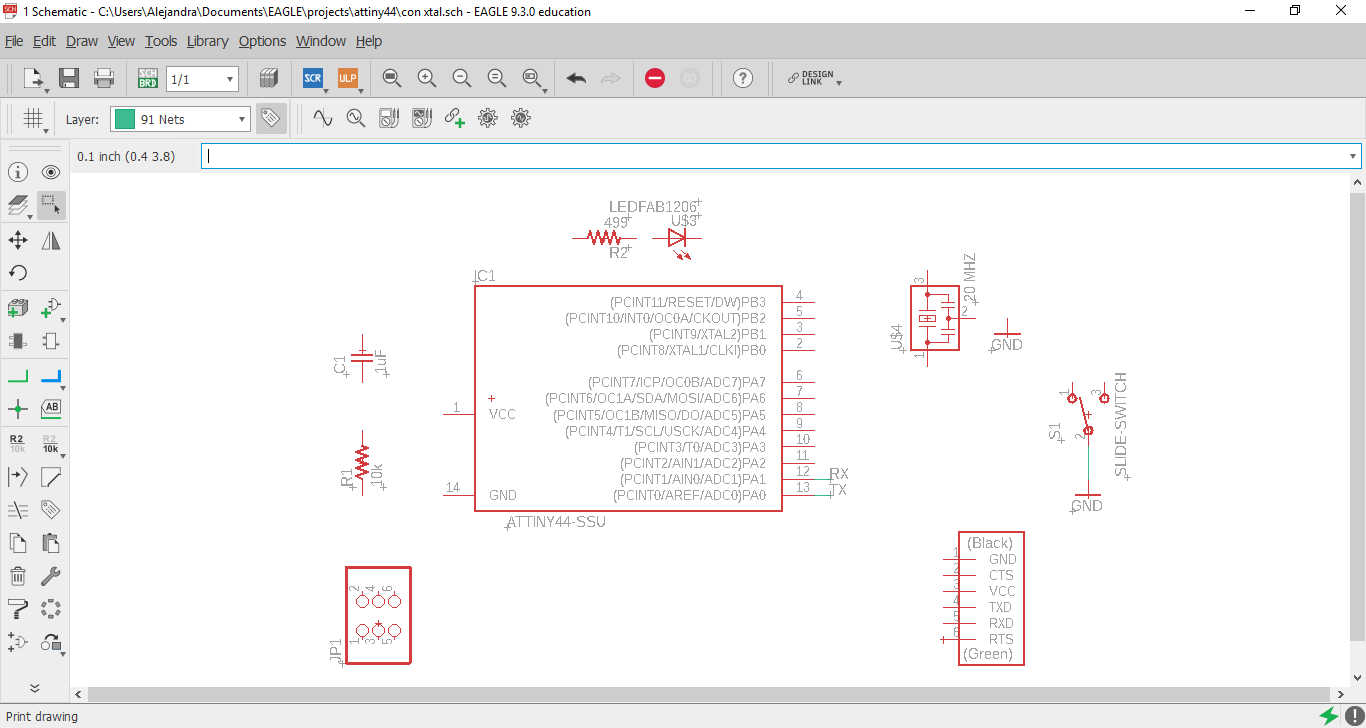
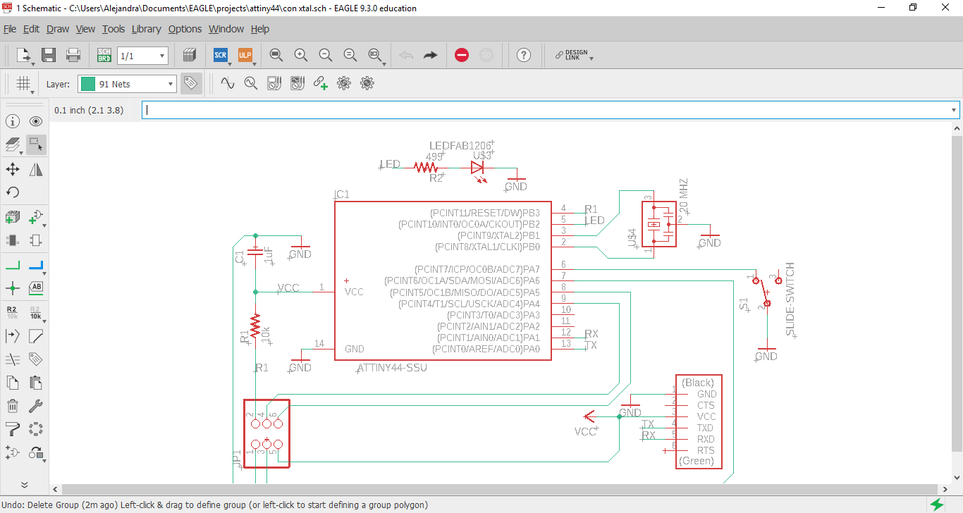
Connections
Then I started making the connections carefully. I didn't want to connect two components that weren't supposed to be connected or to alter the order of the pins in one of the headers. (One of my classmates made the connection of the FTDI header in a different order and this issue wasn't noticed until it was programming time)
This part is very important, it is not only that your board wouldn't be working properly, this could is fixable, but also a short circuit. The micro-controller wouldn't work anymore.
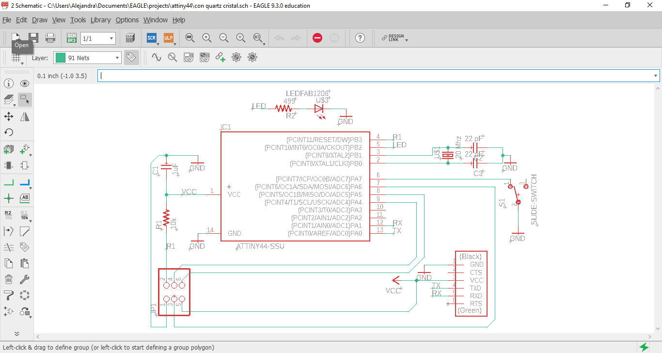
As I described before I made a mistake between the resonator and the crystal. At this point I wasn't sure if it was my mistake or the person in charge of the components cabinet gave me a quarts crystal because they didn't have any resonators left. I think now it was an issue between terms and how some components are usually called in Spanish.
I read the Attiny44 datasheet and realized that I would be able to use what I had, I just needed two extra capacitors. This meant that either I choose to use the resonator or the crystal I didn't have all the components I needed and also I forgot a resistor for the led.
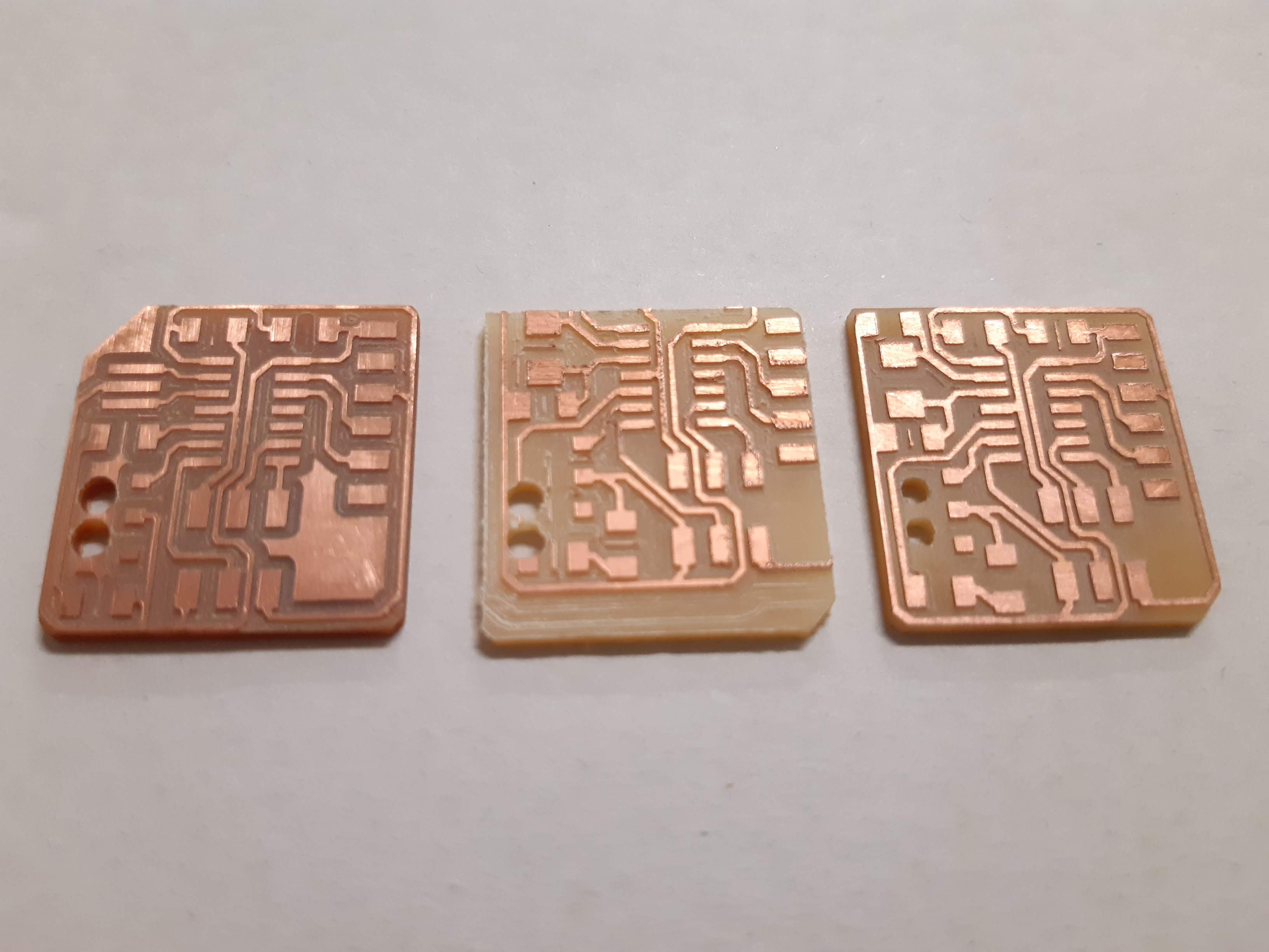
This is why I decided to design and mill the two versions of this board.
The one above has the resonator and the one below has the quartz crystal.
board
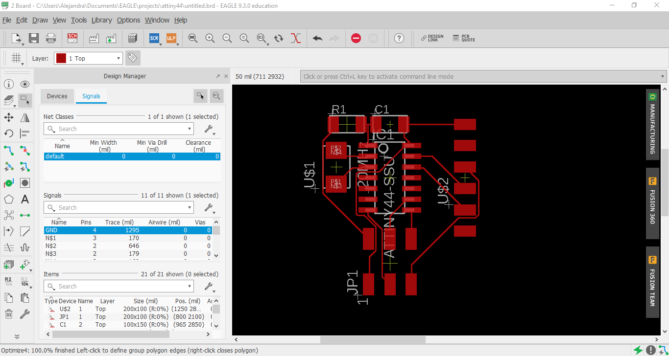
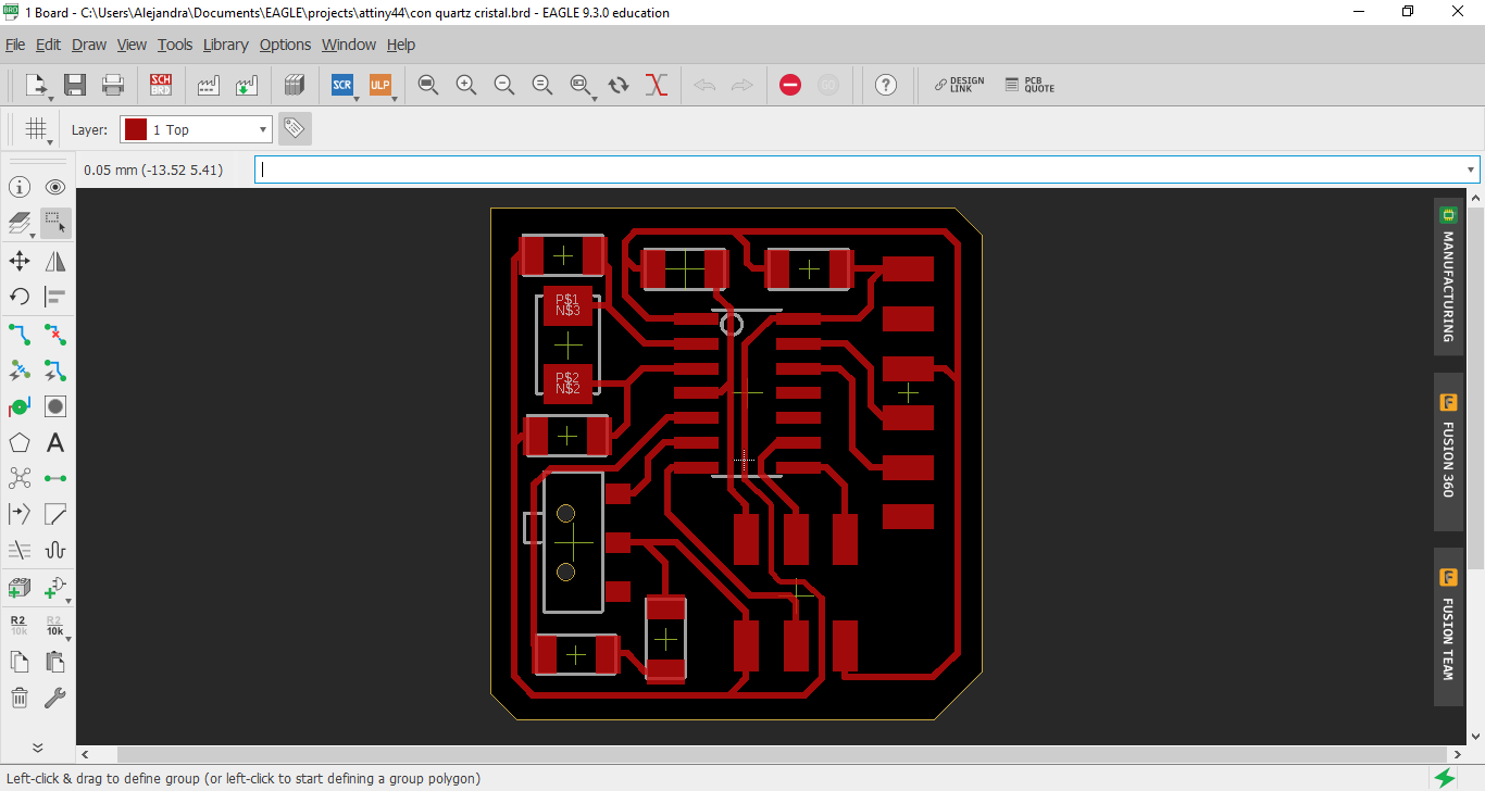
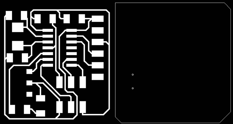
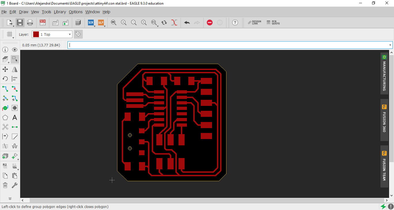
Eagle works with two archives simultaneously one is the schematic part which I've already shown you and the other is the board. The board is PCB layout, this is where you can arrange or place the components and create the routes that connects them in the way they will actually be on the PCB.
This feature of the software makes different important things. It draws and defines the surface with copper where the components will be soldered and also creates the routes that makes connections between each component.
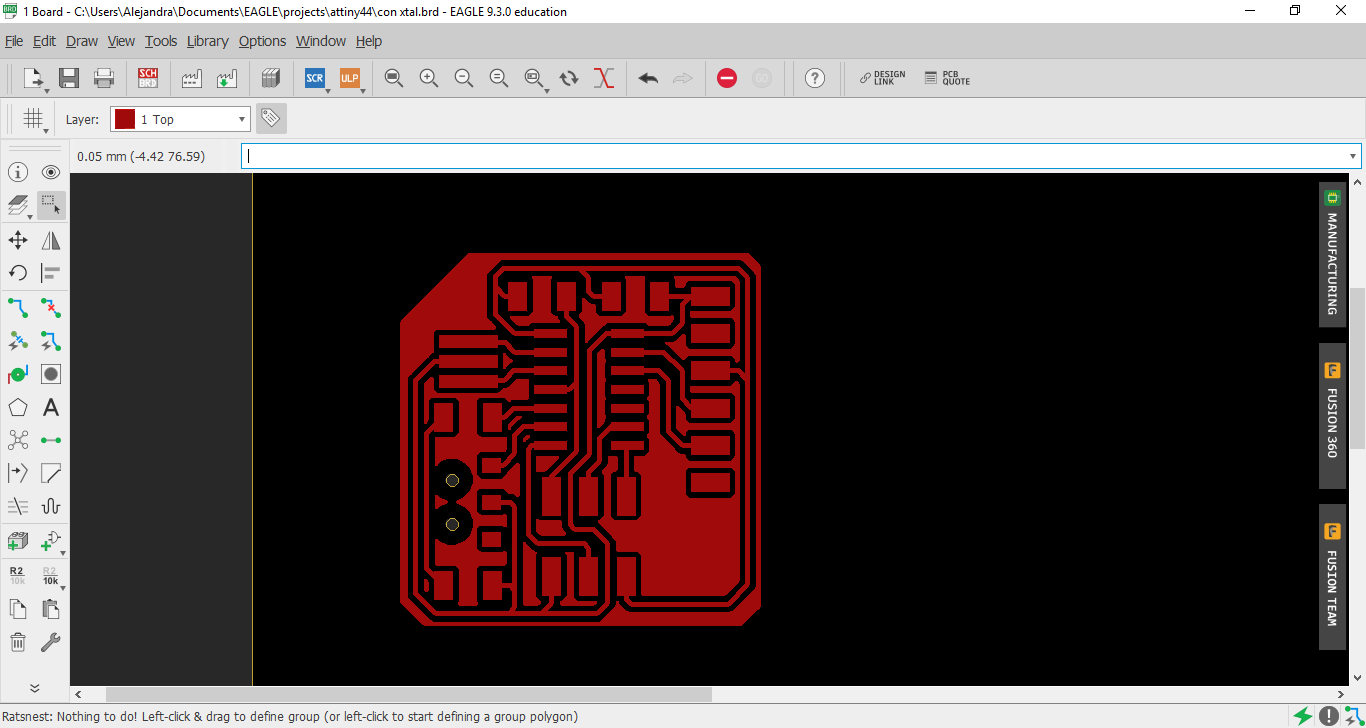
Routes design
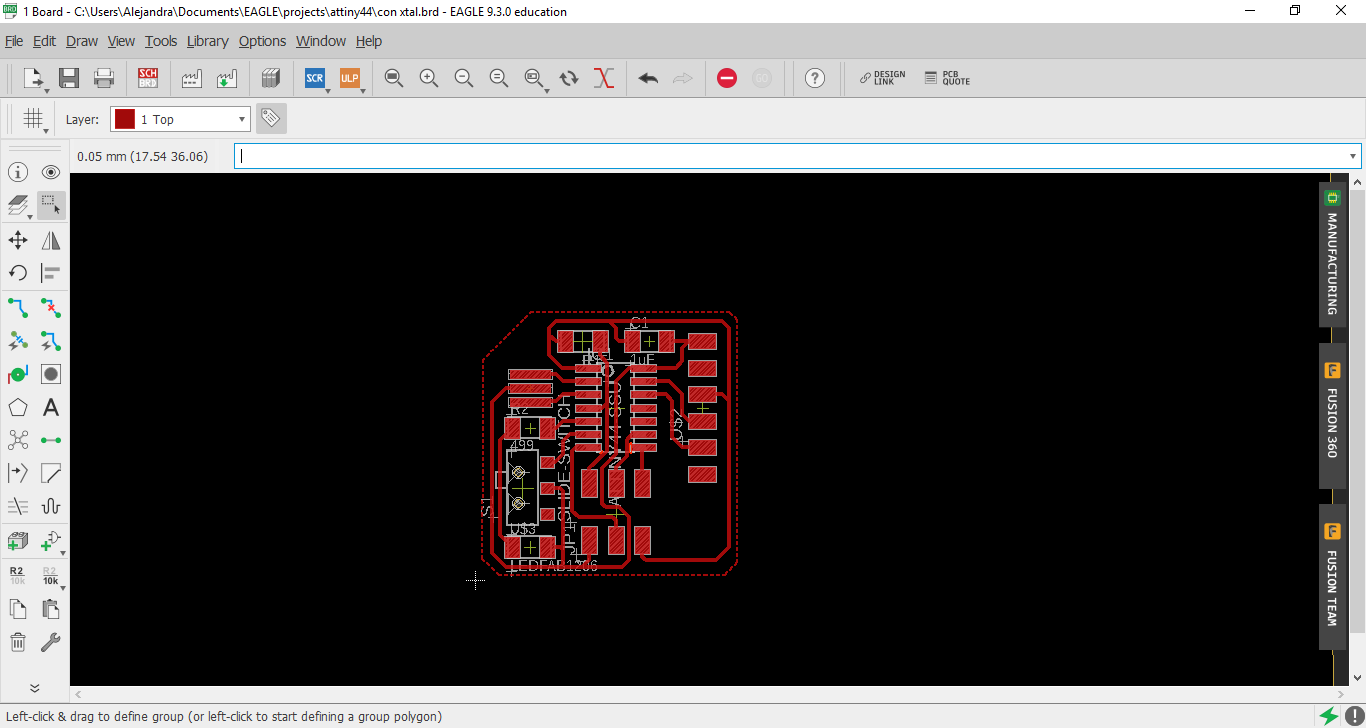
Drawing the routes is very easy, this software is very friendly. You can place the components manually and then there is an option called auto-route, which I tried.
As you can see here I experimented with it before placing the switch and led.
The auto-route was not a good suit for me. I even tried to use it as a guide but I ended up drawing all the routes from scratch.
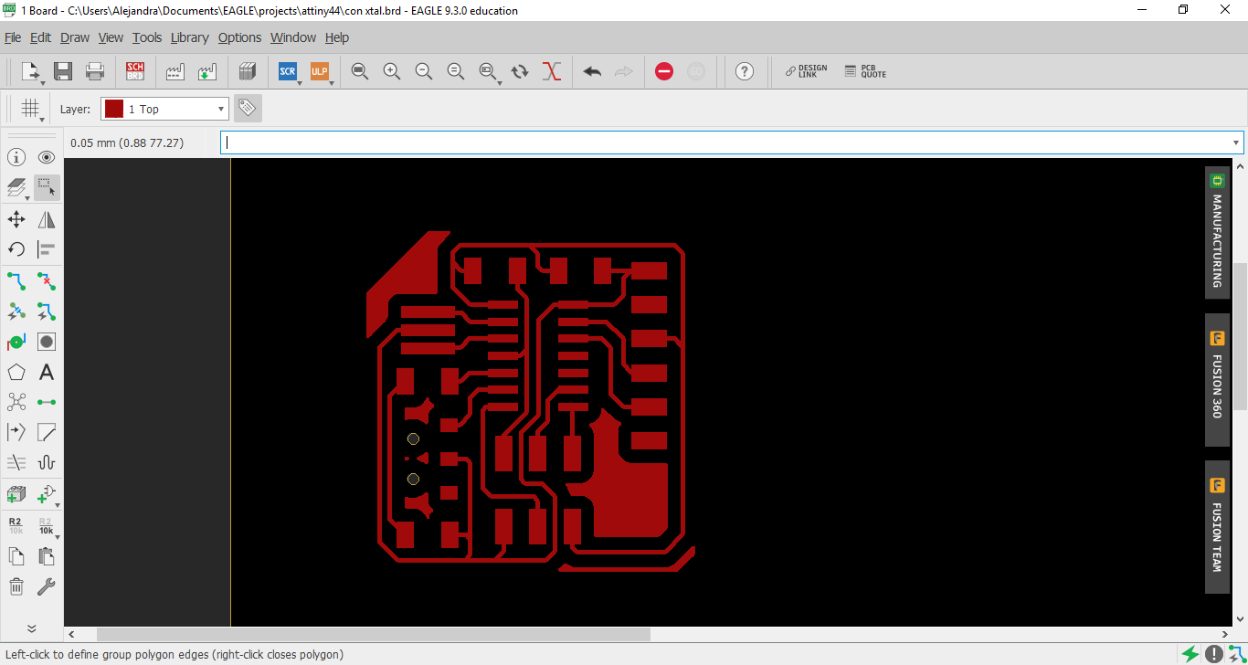
Route's width
The path thickness is very important, it determines the quantity of material we are going to take of with the milling machine, it also determines the space between each path that may be impossible to make if your tool isn't thin enough, etc.
So the first thing I did was define a new thickness to the traces. I selected all the routes and ran the command change width 0.3 pressed enter, then right clicked on the board and selected change group. You can put the value according to what you need or prefer on your routes.
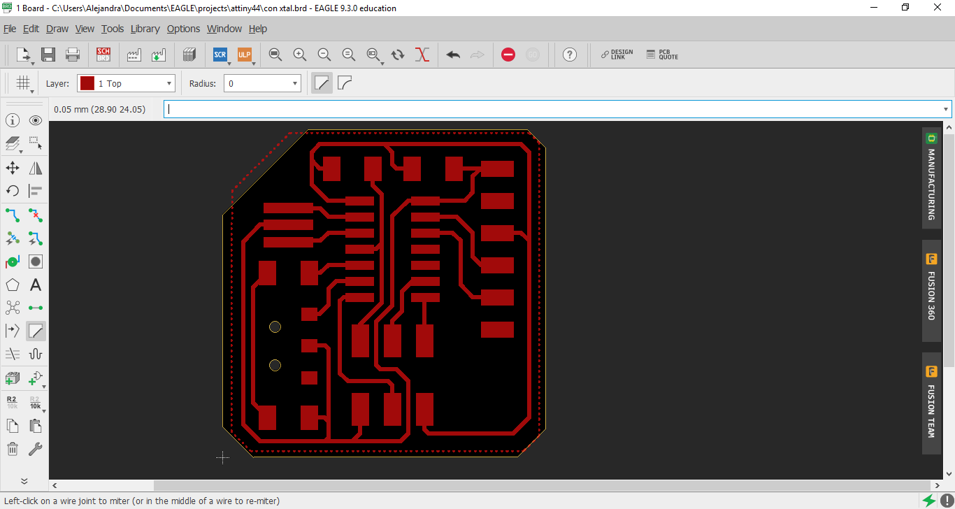
PCB Outline
After this I wanted to define the outline so I used the command polygon to create my board's form.
PCB outline is the actual size of the board. If you are using a board for just a test it may be not so important, but if you are fitting the board to a project, like a device or machine, you should consider this a very important step
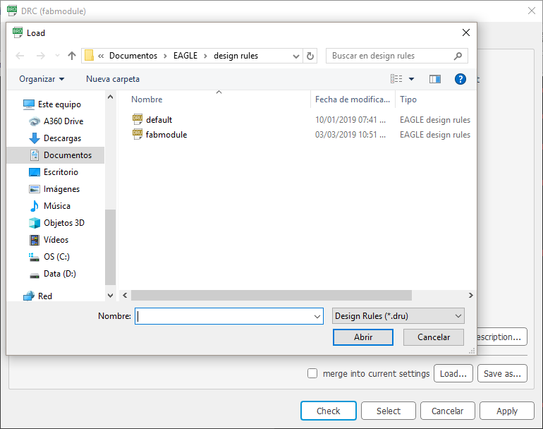
design rules checker
Now I had all defined so I ran the DRC. Again you can find the DRC I used here, it is the fabmodule.dru. DRC is important, because with this tool you will know if your design is machinable depending of the tool you are going to be using. If you don't run this correctly, your machine may skip some passes,and trust me, you don't want that.
Once you have the file needed inside the desgin rules folder for eagle you just have to go to Tools>DRC>Load, select the file and then click on Check.
I had only one problematic part. It took a little while but it was completely fixable. I just needed to move the routes a little bit.
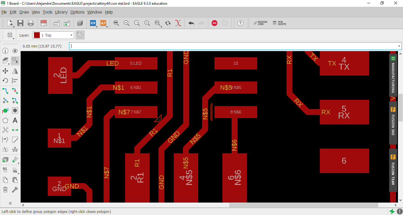
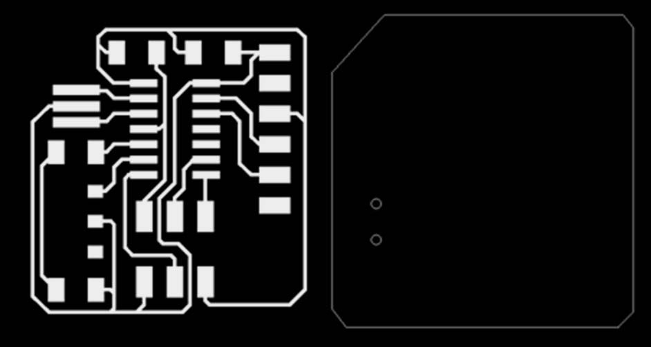
Next I used the command Rat, it started looking like the final milled board.
I ran the command change iso 1, pressed enter and again right click and "change group". Now it was like a milled board with 4 passes offset.
I realized the outlined that I needed wasn't there anymore. These two last steps are mostly useful when you are going to print this design and make the board with acid or if you are going to mill your board using Flatcam. Also it is very useful to make the GND connections. If you name your polygon "GND" and then run the "Ratsnet" command all of the GND connections will be attached to the remaining copper, that is to say, to the parts that are not withdrawed when machining.
Finally, I learned how to define the outline. I reduced the size of the background and edited the corners. I realized about this when trying to export the first png archive, activating and deactivating some layers.
Generating PNG file
To generate the png file that we will use to mill our PCBs we need to export image. It is important that we choose the Monochrome option, change resolution to 500dpi.
For the layers we need to have just the Top layer activated for the traces and the Dimension layer for the outline.
I repeated the same steps for the second version of the board.
fabricating the board
Milling and soldering
Milling
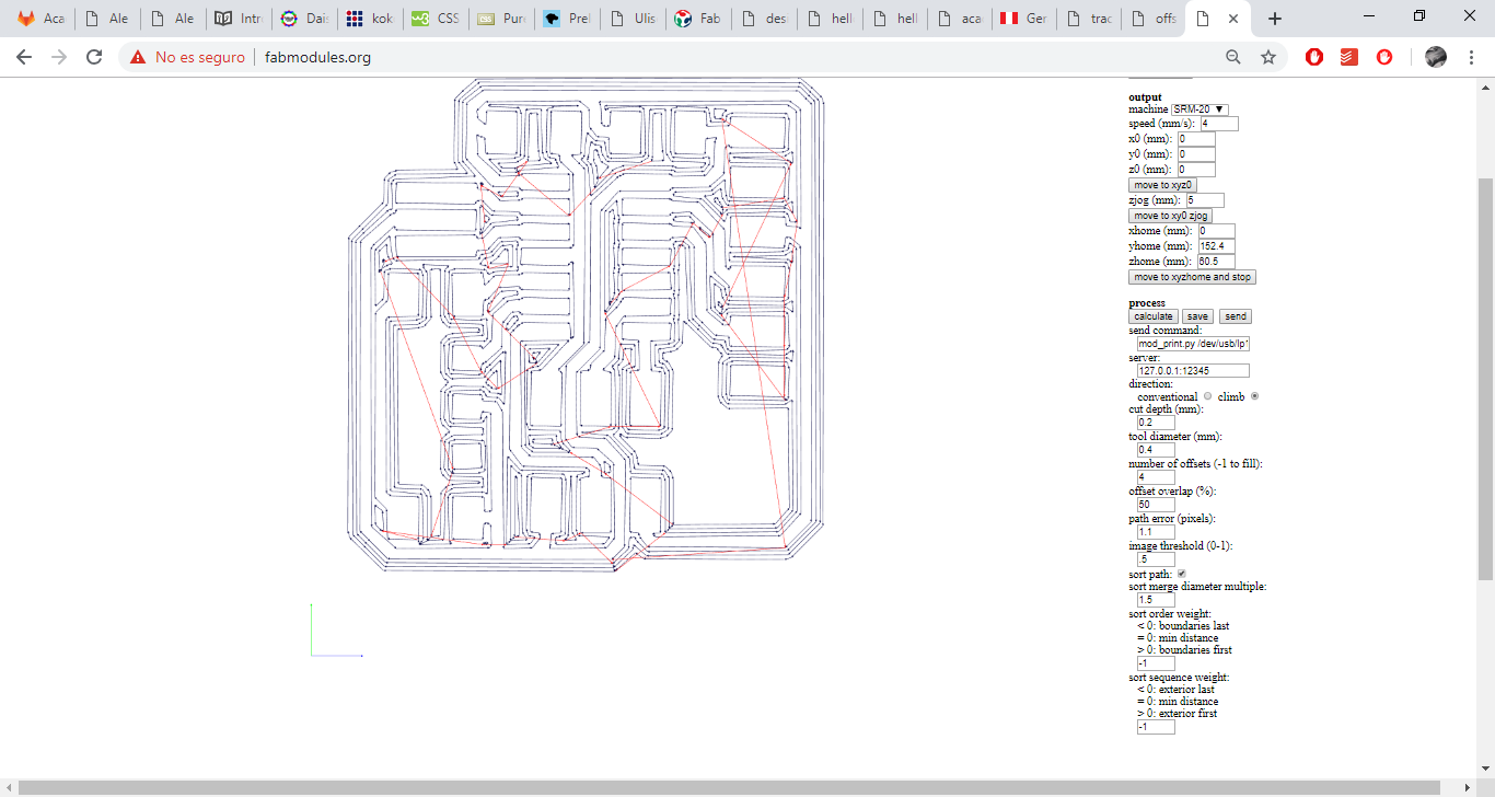
I used the fabmodules again as I did in week 5, you can check that up for more specific information about this part of the process.
For this first PCB I used a 0.2 cut depth and 4 offset passes.
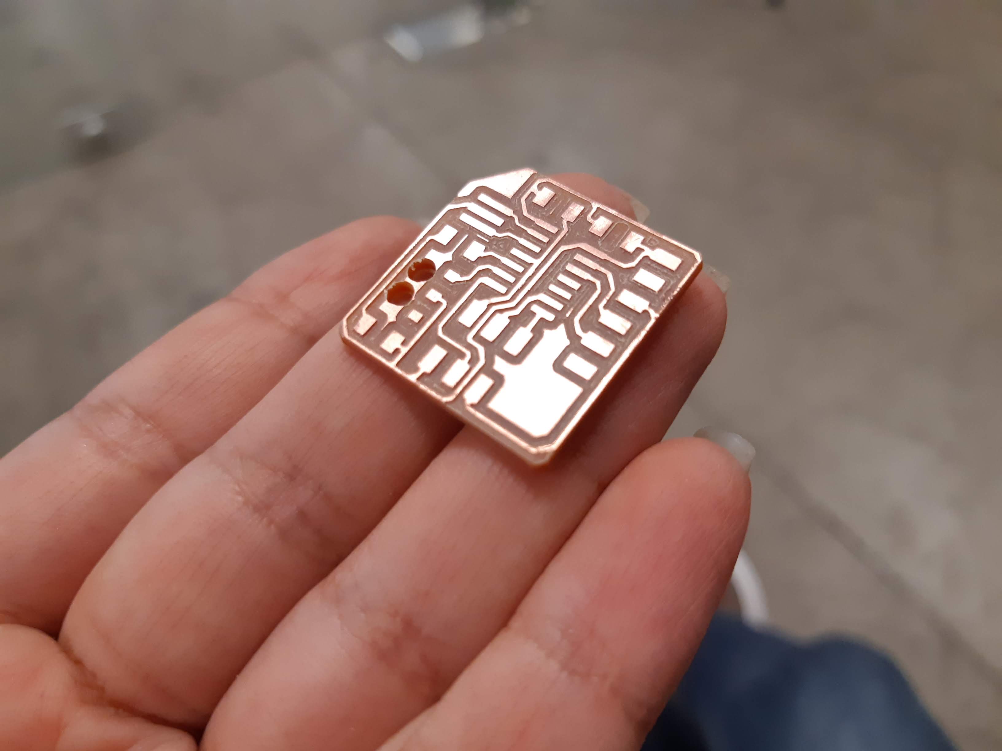
It worked perfectly.
I did the same with the second board but with -1 offset.
It didn't turn out well. I made a mistake when editing the png file in photoshop and it turned out like this.
As I was going to edit again the images I decided to edit the size of the holes for the switch.
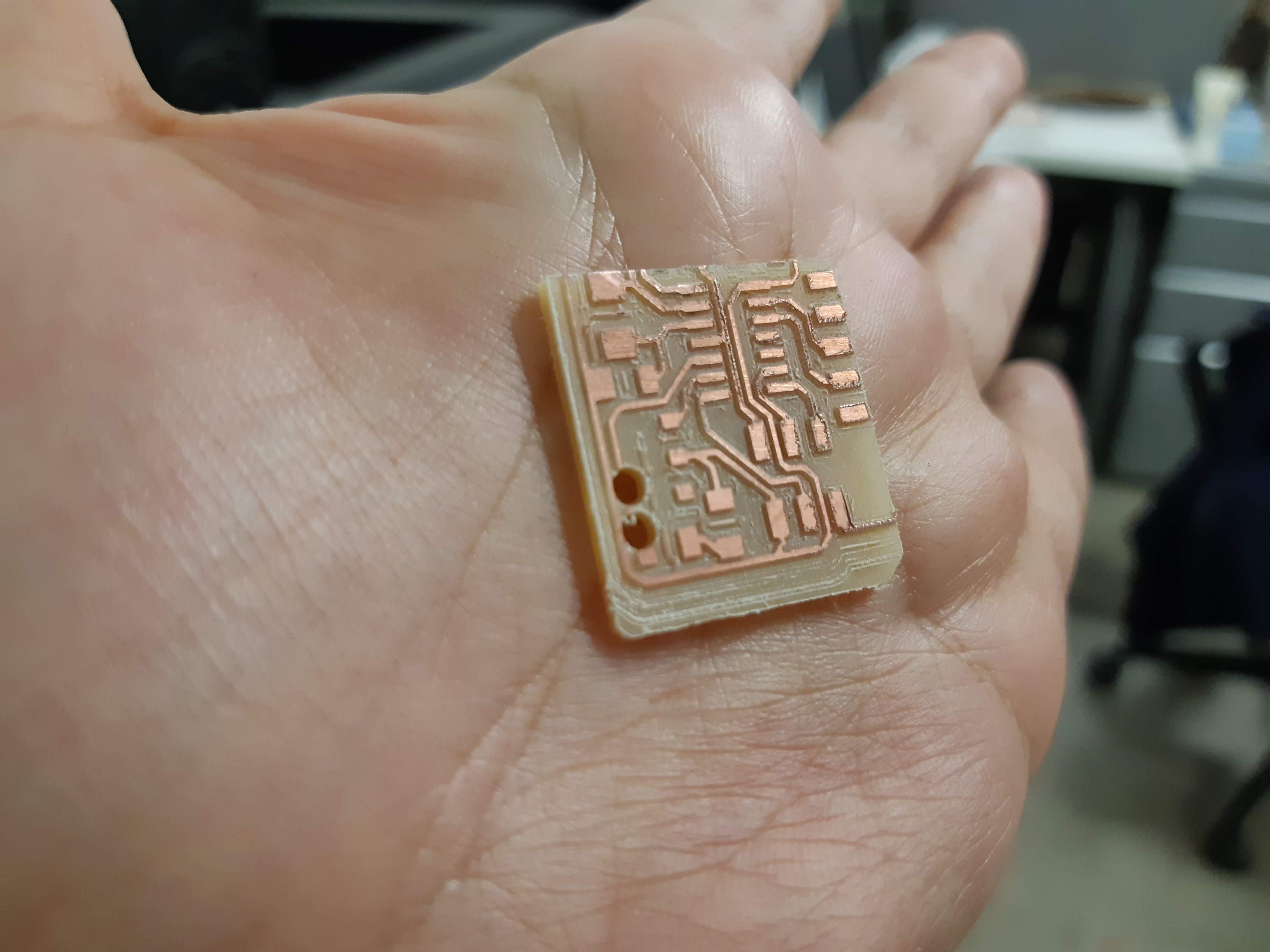
This time It came out a lot better.
Soldering
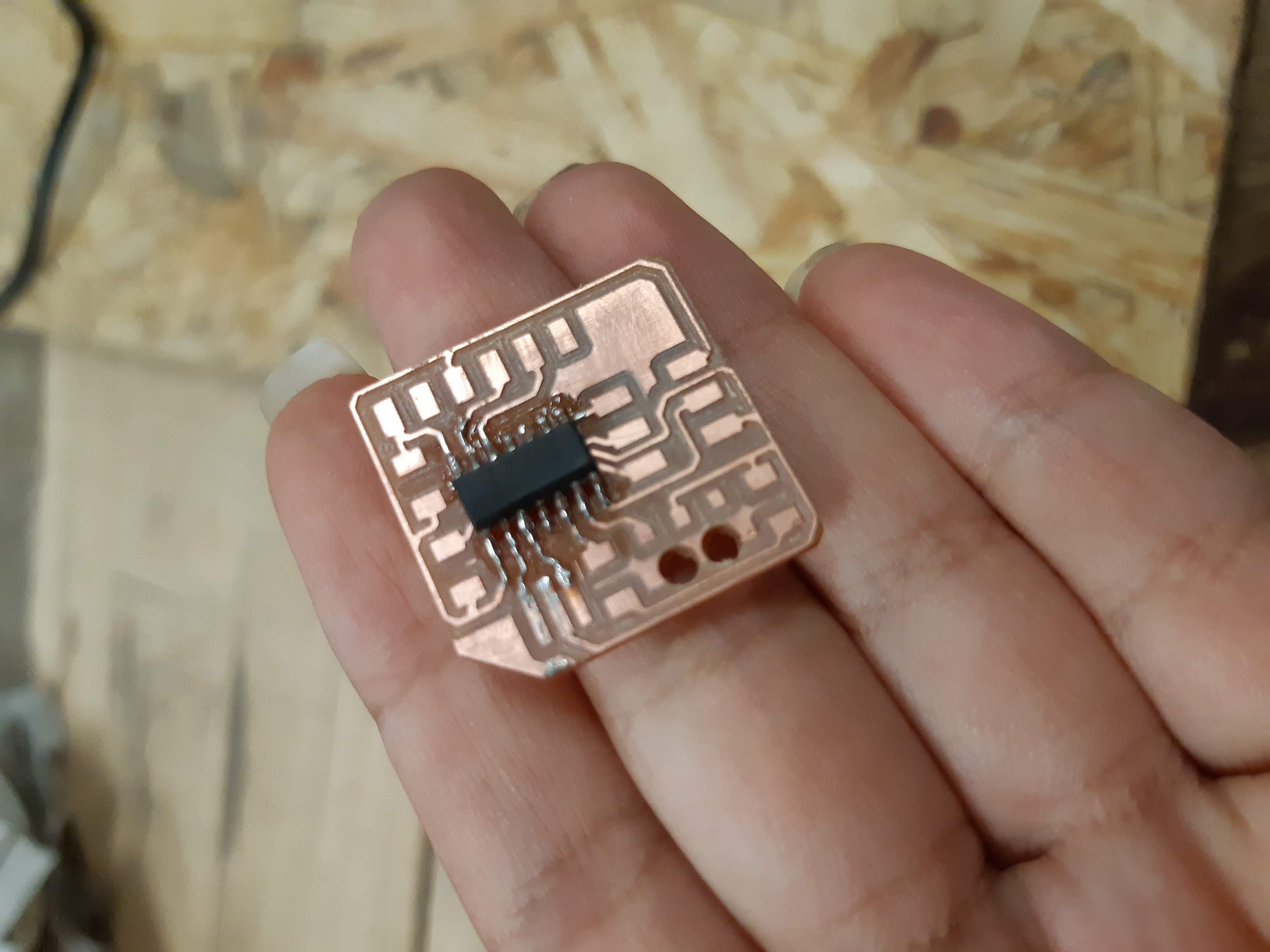
I started with the microcontroler
Then I continued with the stuff I currently had with me.
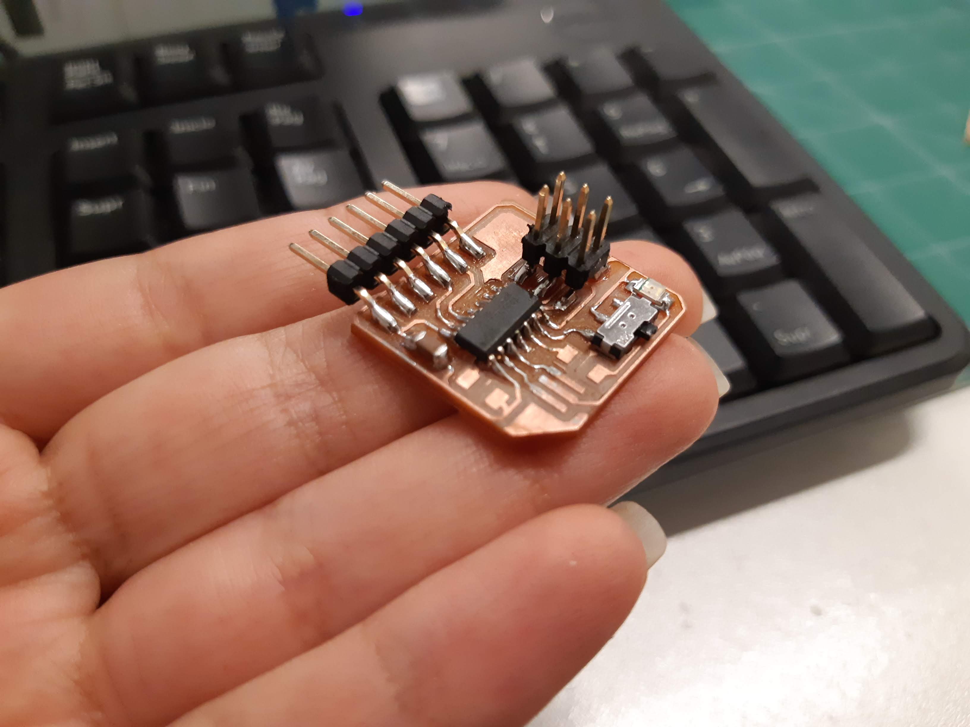
Finally I got the components I was missing, but had two issues.
The first one was that I tried to solder the resonator with the wrong steps order, I put the tin on the copper surface to be soldered but I did that at the 3 contact surfaces at the same time. When trying to fix it one of the traces started to detach from the board. I was able to solved it and make it work without adding some cables. If you see in the image, the resonator is a little bit to the side because I soldered it to where the path was still attached to the board, I was extremely careful that the traces do not touch each other, and check that with the multimeter.
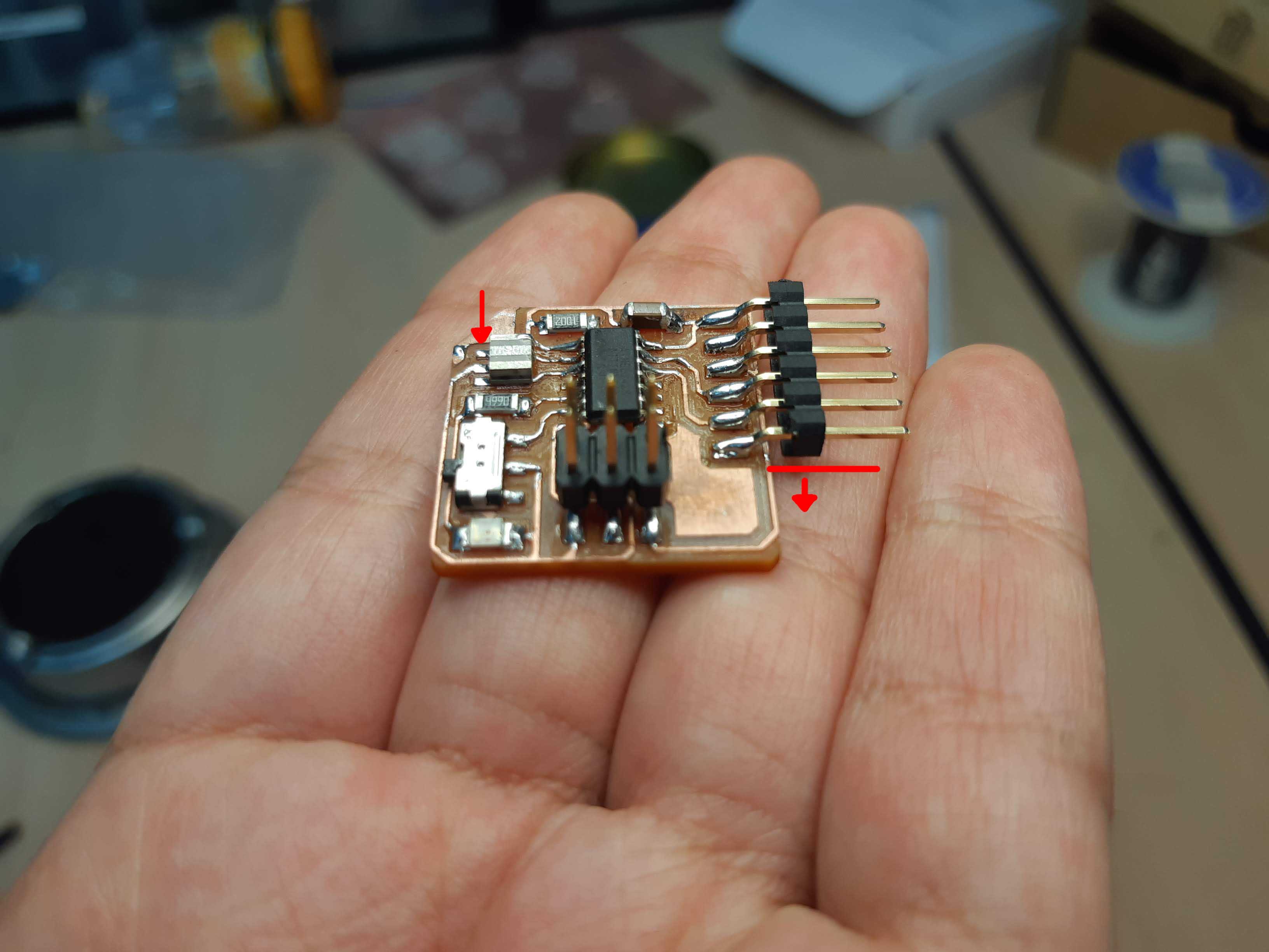
The second issue was actually a design problem. I didn't realized that the FTDI header needed some space for it to rest, all I wanted was to optimize space as much as I could.
Unfortunately the FTDI was floating and had the risk to breaking or going out.
That is why I redesigned and edited the board a little bit, in case something went wrong with this first one.
What was achieved?
I learned that it is important to know beforehand the logic of our board and what will we need, it is important that we just check the information available.
I also learned and understand a little better the logic of the components in a board. I could make it work with that information.
What wasn't achieved?
I still had some issues when soldering the components and also with the physical result of my design. But I'm sure those are things I'll get better at with practice.