Input devices
1. Weekly Brief Summary
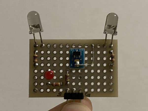
I incorporated various input devices into the obi-dome that I made in the Final Project. I used a photo transistor, a sound sensor, and an accelerometer. You can see how they work and how to program them in Breadboard Prototyping & Programming on the Final Project page. After that, I created a circuit diagram in EAGLE and used SRM-20 to cut the board.
2. Weekly Assignment Requirement
The second half of the Fab Academy programme is designed to build on the previous weeks. You will be synthesising information and implementing skills that you were introduced to in the first half of the programme and encouraged to integrate these into your final project proposal.
Group assignment
- Probe an input device(s)’s analog and digital signals
- Document your work (in a group or individually)
Individual assignment - Measure something: add a sensor to a microcontroller board that you have designed and read it.
Learning outcomes
- Demonstrate workflows used in sensing something with input device(s) and MCU board
Have you?
- Linked to the group assignment page
- Documented what you learned from interfacing an input device(s) to microcontroller and how the physical property relates to the measured results
- Documented your design and fabrication process or linked to previous examples.
- Explained the programming process/es you used
- Explained problems and how you fixed them
- Included original design files and source code
- Included a ‘hero shot/video’ of your board
3. Group Assignment Link
Kamakura Group Assignment Week9
4. Description of Assignment Work
Creating a circuit in EAGLE
Based on the breadboard circuit we created, we selected surface-mounted sensors and other components to be used.
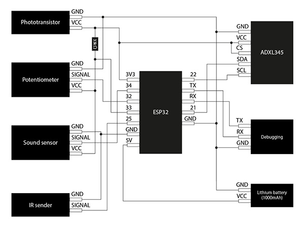
breadboard diagram
① ESP32
I decided to use the surface-mounted Wi-Fi module ESP-WROOM-32 for the ESP32.
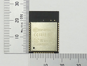
data sheet
- Main Specifications
| Function | Details |
|---|---|
| Power supply voltage | 2.2V~3.6V |
| SRAM | 520KB |
| WiFi | 802.11 b/g/n |
| Bluetooth | v4.2 |
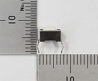
I also have some new components based on [Barduino 2.0], which implements the ESP32. When writing a program to the ESP32 using an Arduino, when you see [Connecting…], press the reset button and when you see [Leaving… Hard resetting via RTS pin], press the switch Switch to run mode and press the reset button. So you need two [tact switch], which is necessary to write the program.
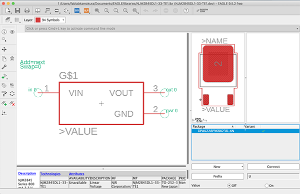
In addition, a regulator [NJM2845DL1-33] is available to control the output voltage and current so that it is always constant.
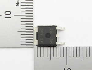
data sheet
Finally, we have an LED for the ESP32 debugging.
- Parts used
| Function | Details | Number |
|---|---|---|
| ESP32 | Wi-Fi module ESP-WROOM-32 | 1 |
| Switch | tact switch | 2 |
| Regulator | NJM2845DL1-33 | 1 |
| LED(Red) | Red Chip LED [1608] OSHR1608 | 1 |
| Resistor ⑴ | 100Ω | 2 |
| Resistor ⑵ | 10kΩ | 2 |
| Resistor ⑶ | 2.2kΩ | 2 |
| Capacitor ⑴ | 0.1μF | 2 |
| Capacitor ⑵ | 10μF | 2 |
| Programming Writing | 4 pin header | 1 |
Footprint
I used [ESP-WROOM-32], which is in [ESP32.lbr]. I couldn’t find the regulator footprint on the web, so I made my own using EAGLE, using the datasheet as a reference.
I used [TACT_SWITCH] in [fab.lbr] for the TACT switch footprint and [LEDFAB1206] in [eagle_fab.lbr] for the LED(Red) footprint. I also used [R1206FAB] in [eagle_fab.lbr] for the resistor footprint and [C1206FAB] in [eagle_fab.lbr] for the capacitor. I decided to use a 4-pin pin header to write the program, so I used four [PINHD-1×1] in [adafruit.lbr] for its pads.
② Infrared Transmitter
For the infrared transmitter, we decided to use a partial switch from the device used for the breadboard circuitry to a surface mount component.
schematic
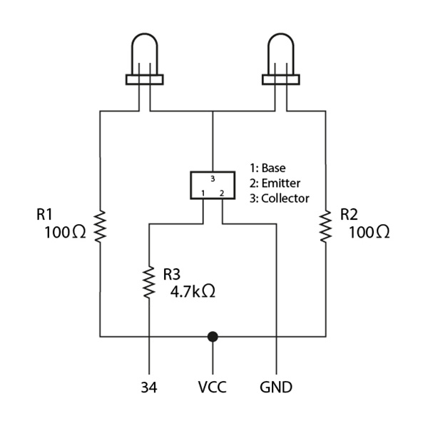
- Parts used
| Function | Details | Number |
|---|---|---|
| Infrared Transmitter | 5mm Infrared LED 940nm OSI5LA5453B | 2 |
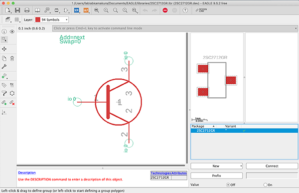
| Chip transistor | 2SC2712-GR | 1 |
| Resistor ⑴ | 100Ω | 2 |
| Resistor ⑵ | 4.7kΩ | 1 |
Footprint
I couldn’t find a footprint for the [2SC2712-GR] on the web, so I made my own using EAGLE, using the datasheet as a reference. I also used [R1206FAB] in [eagle_fab.lbr] for the resistor footprint and [PINHD-1×1] in [adafruit.lbr] for the LED pads.
data sheet
↓
③ Phototransistor
Phototransistor [Phototransistor 3mm round type 940nm L-31ROPT1C] used for breadboard circuit.
dateseet
- Main Specifications
| Function | Details |
|---|---|
| short legs | collector(C) |
| long legs | emitter(E) |
| feature | ・It has a large lens and high sensitivity. ・Fast response time. |
- Parts used
| Function | Details | Number |
|---|---|---|
| Phototransistor | Phototransistor 3mm round type 940nm L-31ROPT1C | 1 |
| Resistor | 33kΩ | 2 |
footprint
I used [R1206FAB] in [eagle_fab.lbr] for the Resistor footprint and [PINHD-1×1] in [adafruit.lbr] for the LED pads.
④ Sound Sensor
For the sound sensor, we decided to use a partial switch from the device used for the breadboard circuitry to a surface mount component.
schematic
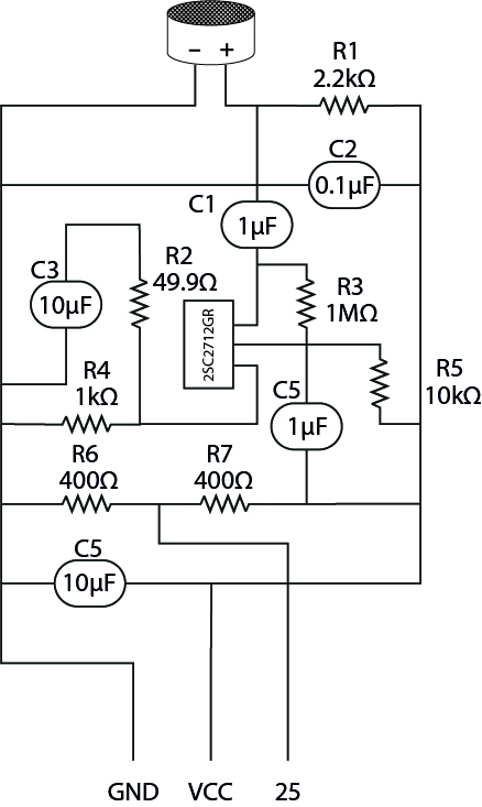
- Parts used
| Function | Details | Number |
|---|---|---|
| Microphone sensor | [Electret Condenser Microphone (ECM) WM-61A or equivalent with lead pin] | 1 |
| chip transistor | 2SC2712-GR | 1 |
| Resistor ⑴ | 400Ω | 2 |
| Resistor ⑵ | 49.9Ω | 1 |
| Resistor ⑶ | 10kΩ | 1 |
| Resistor ⑷ | 1MΩ | 1 |
| Resistor ⑸ | 1kΩ | 1 |
| Resistor ⑹ | 2.2kΩ | 1 |
| capacitor ⑴ | 0.1μF | 1 |
| capacitor ⑵ | 10μF | 2 |
| capacitor ⑶ | 1μF | 2 |
footprint
I made my own [2SC2712-GR] footprint, [R1206FAB] in [eagle_fab.lbr] in the Resistor footprint, [Electret Condenser Microphone (ECM) WM-61A or equivalent with I used [PINHD-1×1] in [adafruit.lbr] for the [lead pin] pad.
⑤ Accelerometer ADXL345
I decided to use the [ADXL345] used for the breadboard circuitry as it is for the Accelerometer.
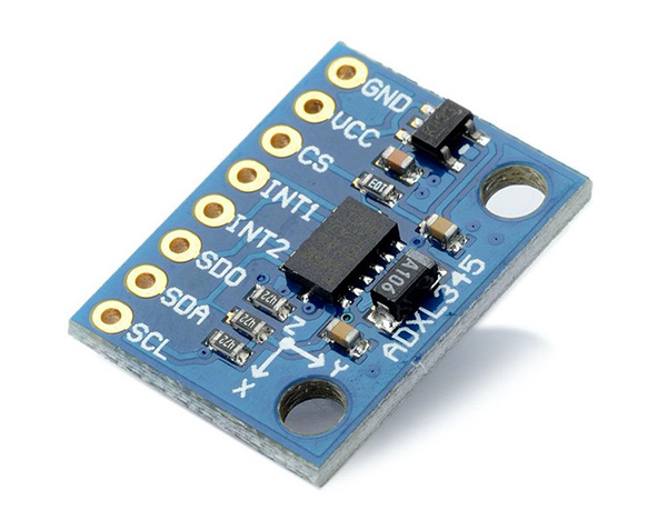
data sheet
- Parts used
| Function | Details | Number |
|---|---|---|
| Accelerometer | ADXL345 | 1 |
| Connect | 6 pin header | 1 |
footprint
I decided to use a 6-pin pin header to plug the ADXL345 directly into the board. So I used the [PINHD-1×6CB] in [adafruit.lbr] for that pad.
⑥ Power Supply
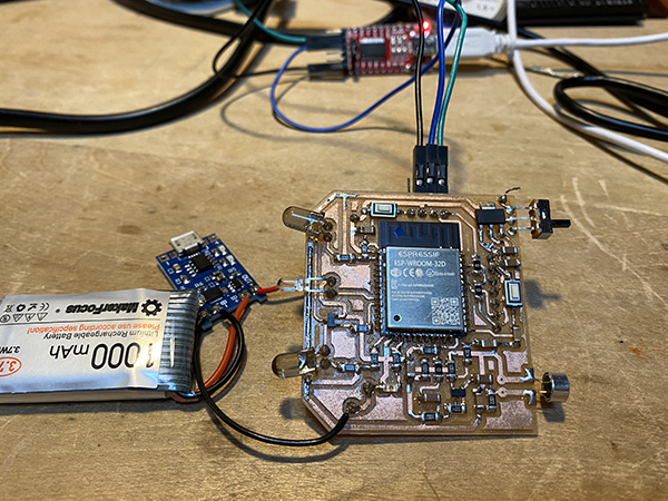
I used [Rechargeable lithium battery(1000mAh)] and charging circuit [Lithium Ion Charging Module_TP4056] for breadboard circuit. And I used [Slide switch for boards SS-12D00-G5] as a power switch.
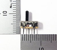
dateseet
footprint
I decided to create the footprint of the slide switch in [Adobe Illustrator] instead of EAGLE as I did when I created the pattern diagram for the infrared receiver in [Board B].
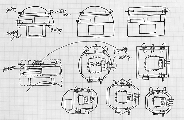
Consideration of board design
Before I worked on EAGLE, I considered the design of the board to be produced. When you look at the device from the front, you must place the infrared transmitter and phototransistor at the top. Then I thought it would fit together as a design by placing the microphone sensor, power switch, and charging circuit underneath the device so that it could be operated.
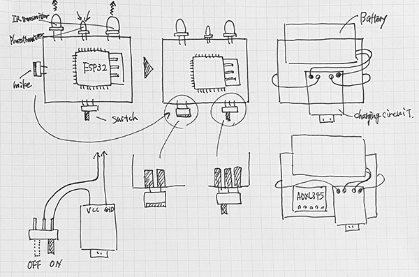
The device was originally going to be a round design, but we felt that we needed to consider a square or hexagonal design due to the space available on the board. We don’t plan to make the device itself too large, but rather we want it to be less than 700mm in width and length, and less than 500mm in height.
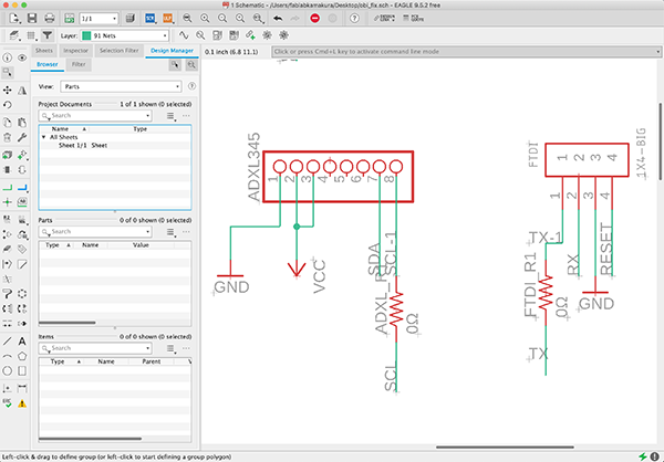
Creating a [Schematic]
I was able to prepare the symbols and footprint data for the parts used on the obi-dome side, so I created a schematic using EAGLE.
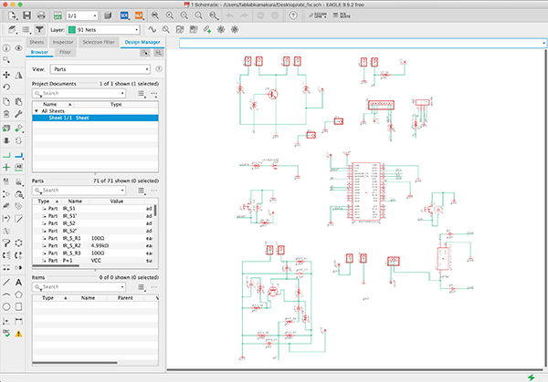
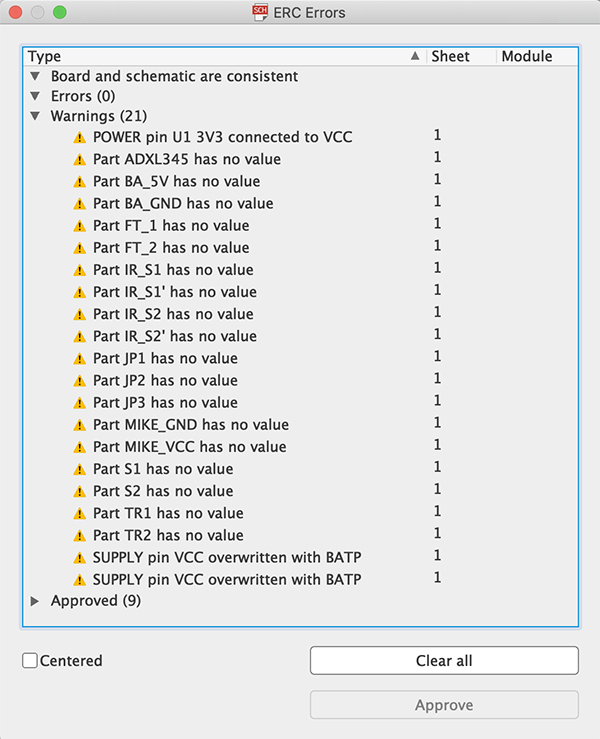
The warning [Part xxx has no value] is displayed, but I ignored it because it’s not necessary to make the board we’re going to create this time.
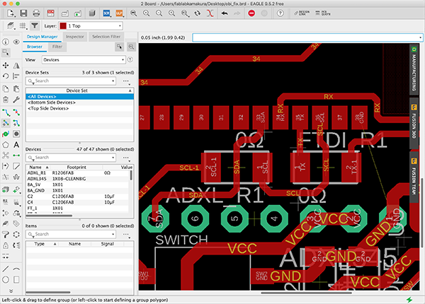
Creating the [Board]
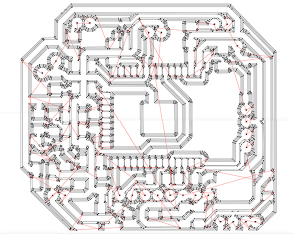
The next step is to create the board diagram. The final board design for [Board B] looks like this.
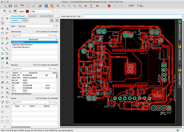
This time, unlike [Board A], the width of the solid bars connected to the power supply such as GND and VCC is set to [0.032] inch. This treatment is to make the resistor value low.
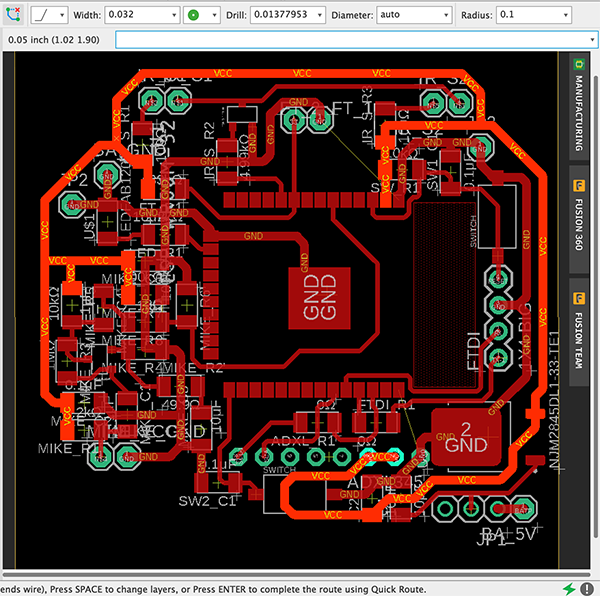
Also, since there were quite a few parts to be used in this project, there were parts that could not be connected. I thought about using [0kΩ] to connect wires by passing a solid underneath the components. So I added [0kΩ] in the [Schematic] section.
↓
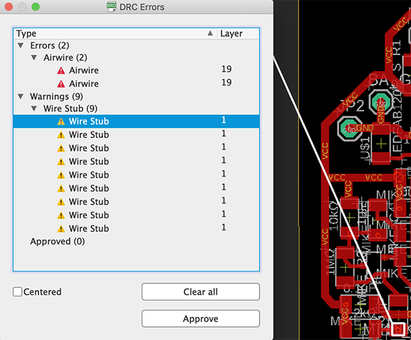
Lastly, I used the [DRC] to check the spacing between the wires. There are some parts of the pattern that are not connected, but this is not a problem as I used tin plated wires to connect these parts.
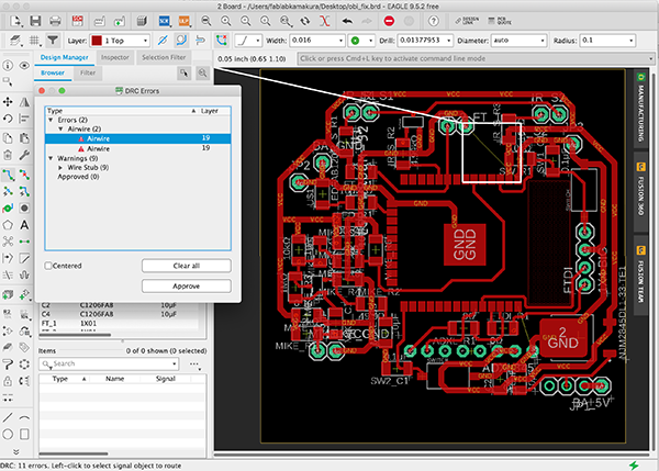
I also found 9 extra solids in [Wire Stub], but I ignored them as they were warnings that I didn’t need to worry about, especially when exporting the pattern diagram as an image.
Corrections in [Adobe Illustrator]
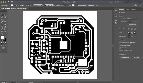
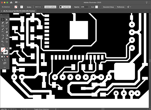
I edited the [DXF] file exported by EAGLE in the same way as [Substrate A] by using [Adobe Illustrator]. In the final pattern, I reduced the extra space as much as possible and made the corners as small as possible.
What I modified here is the size of the footprint of the ESP32…the footprint is too wide to be machined with the pattern created by EAGLE, so I made a [0.016]-inch space for a solid block.
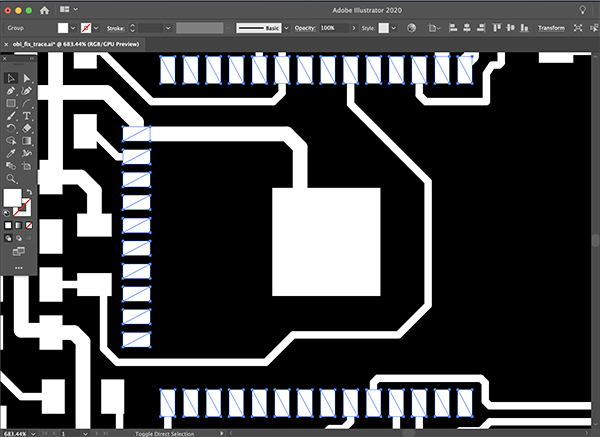
An additional thing I created was a large pad section for the microphone sensor and slide switch, so that it could be adequately secured by just soldering it in place.
The part you are selecting is the part where you drill a hole and connect the wires from the back with tin-plated wire.
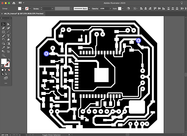
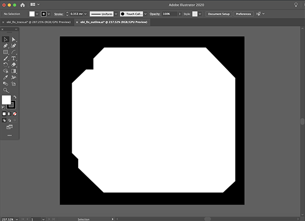
Finally, I created the outline data. I exported the pattern and outline data in the [PNG] file format.
Board production
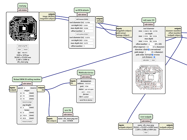
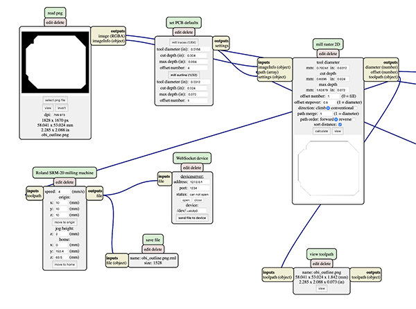
G code generation with Mods
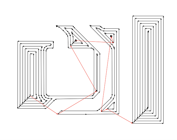
I used the pattern I created, a [PNG] file of outline data to generate the G-code from the mods.
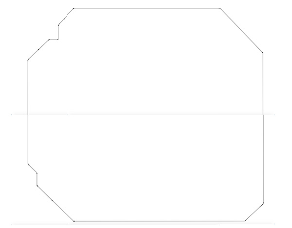
Obi clasp pattern
Obi clasp outline
In the case of the obi clasp side board, I needed to remove the copper foil around the antenna, and I used an ultrasonic cutter as well, but the board was torn up.
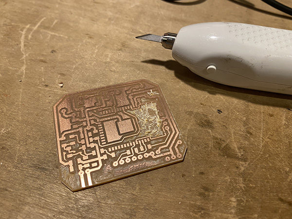
So I created the data to cut around the antenna and the large area to be removed with SRM-20. (Specified in [ESP32 Antenna Processing])
ESP32 Antenna Processing
I decided to write out the cutting data beforehand as cutting data for the part of the cut board where the copper foil was removed using the ultrasonic cutter. I used [Adobe Illustrator] to create the data.
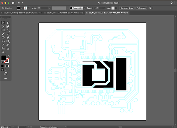
antenna trace
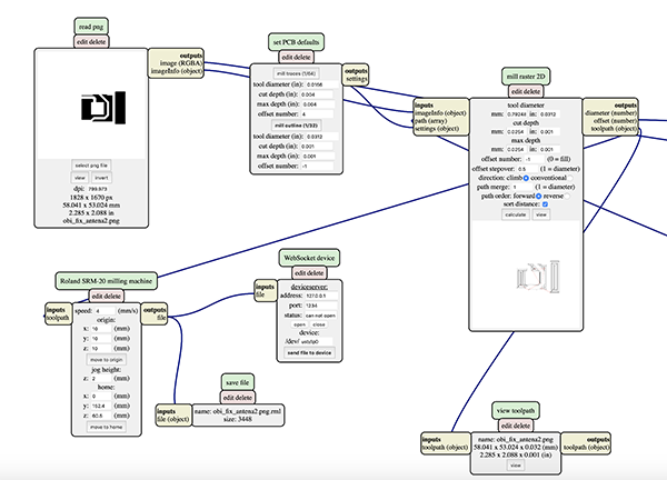
In order to cut all the parts you want to remove, you need to make the following settings. This will cut the copper foil in the excess antenna area.
- cut depth: 0.01 inch (0.254 mm)
- max depth: 0.01 inch (0.254 mm)
- offset number: -1
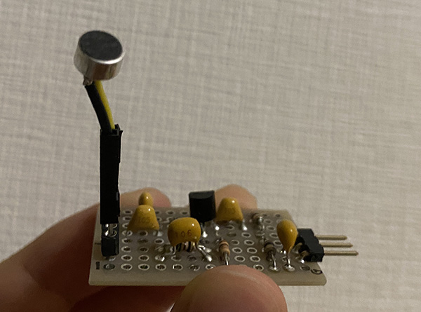
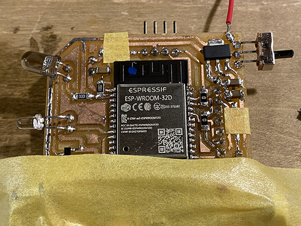
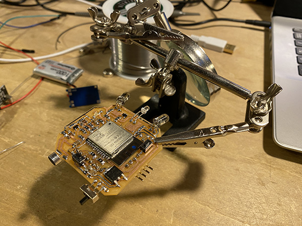
Soldering
There are many resistors and capacitors on the obi clasp side of the board, so it was difficult to solder them. When I soldered the switches for ESP32 program writing, I put masking tape to prevent short circuit.
↓
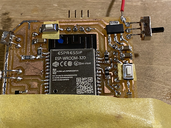
In addition, we used this kind of device to solder through many parts such as the infrared transmitter and the ADXL345, which are soldered through the board.
Emdebbeging Programming
I used a FTDI cable to write the program on the banding side. The pins I connected are GND/TX/RX.
First I wrote a program to light up the LEDs on the ESP32 to make sure there was no problem.
Programminng
//
// hello.ESP32-WROOM.echo.ino
//
// ESP32-WROOM echo hello-world
//
// Neil Gershenfeld 1/6/20
//
// This work may be reproduced, modified, distributed,
// performed, and displayed for any purpose, but must
// acknowledge this project. Copyright is retained and
// must be preserved. The work is provided as is; no
// warranty is provided, and users accept all liability.
//

void setup() {
   Serial.begin(115200);
   }

#define max_buffer 25

void loop() {
   static char chr;
   static char buffer[max_buffer] = {0};
   static int index;
   if (Serial.available()) {
      chr = Serial.read();
      Serial.print("hello.ESP32-WROOM.echo: you typed \"");
      buffer[index++] = chr;
      if (index == (max_buffer-1))
         index = 0;
      Serial.print(buffer);
      Serial.println("\"");
      }
   }
Having verified that the circuitry is OK, I wrote Controller Tapmode [ino] and used the Arduino’s serial monitor and the earring’s breadboard circuitry to check the board for problems.
Debugging with a serial monitor
Debugging with Breadboard Circuits
Usage Scene
I used a 3D printer to print out a model of the circuit board I made, and had a woman in a kimono wear it to photograph the scene of its use. The exterior design of the device is described in Computer Controlled Cutting & Assembly.
Phototransistor mode
When the room is bright, the earrings do not glow, and when the room is dark, the earrings glow.
Switching between lighting modes
You can switch the lighting mode by tapping twice on the obi-dome.
A view of the lighting pattern for the lantern version
This time I created a pattern with a glow-in-the-dark pattern using the earring motif.
4. Links to Files and Code
Footprint
- eagle_fab(Resistor etc…) [lbr]
- fab(tact switch etc…) [lbr]
- adafruit(pin header etc…) [lbr]
- esp32 [lbr]
- NJM2845DL1 33 TE1 [lbr]
- 2SC2712GR [lbr]
- supply1(GND/VCC etc…) [lbr]
EAGLE date
PNG file
![[png]](../../finalproject/files2/obi_trace.png)
![[png]](../../finalproject/files2/obi_outline.png)
![[png]](../../finalproject/files3/obi_antena.png)
RML file
![[rml]](../../finalproject/files3/obi_trace.png.rml)
![[rml]](../../finalproject/files3/obi_outline.png.rml)
![[rml]](../../finalproject/files3/obi_antena.png.rml)
Programming
- hello.ESP32-WROOM.echo [ino]