5. Electronics production
The objective of this week are to first, work with a group to Characterize the design rules for your PCB production process, second, to Make an in-circuit programmer by milling and stuffing the PCB, then test it.
Group Assignment
You can find our group assignment in this link
PCB Board
A printed circuit board (PCB) mechanically supports and electrically connects electrical or electronic components using conductive tracks, pads and other features etched from one or more sheet layers of copper laminated onto and/or between sheet layers of a non-conductive substrate. Components are generally soldered onto the PCB to both electrically connect and mechanically fasten them to it.
PCB milling
To Make an in-circuit programmer first I need to first mill the circuit by using the milling machine, to do this I follow the steps below:
- Go to Fab academy site and chose the circuit that I would like to mill and download the png file.
There are three options available, ISP (AVR), UPDI (AVR 0,1-series), and JTAG (ARM). I decide to go with JTAG (ARM) because in the boot camp I already work with ATtiny 45 due to that choosing ISP (AVR) will be waste of time as I already work with it is microcontroller.
Moving to UPDI (AVR 0,1-series) it seems little bit difficult for a beginner in soldering to make it as the spaces between the line is very small. As a result, I download the JATG (ARM) ATSAMD11C14A png files from fab academy site.

- Convert the png files to rml file that the milling machine could read.
To convert the png file I used Mods you can use Fabmodules also the both provide the same application. In order to convert the png file first open mods>> right click on the empty white space<< programs << open server program << PCB png. This steps will open for you the following set up page and set your settings.
After I was done with making the setups reacquired to convert the files, I download them by clicking on calculate from the mill raster 2D and open the file with Roland software which is the soft ware that we use for the milling machien.
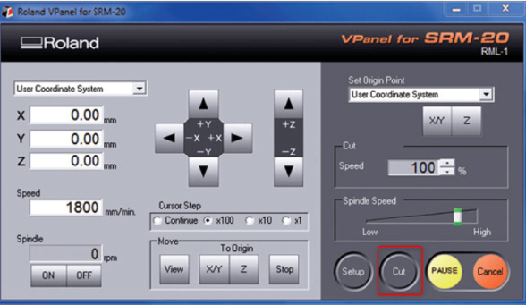
- setup the milling machien
put the copper sheet in the milling machine bed but first try to add a double tape to ensure that the sheet will not move through the process. After finishing this step make sure that the surface of the copper sheet is straight in the machine bed by using the leveling tool. Turn on the machine and insert the milling bit which is (1/64), adjust your x, y, z origins by using the cursor on the software and set up the milling speed. Finally click cut to start milling.
Repeat all the previous steps to mill the interior after milling the traces but I need to change the milling bit to (1/32) and re-origin the starting point by keeping x and y the same and readjust the z point manually.
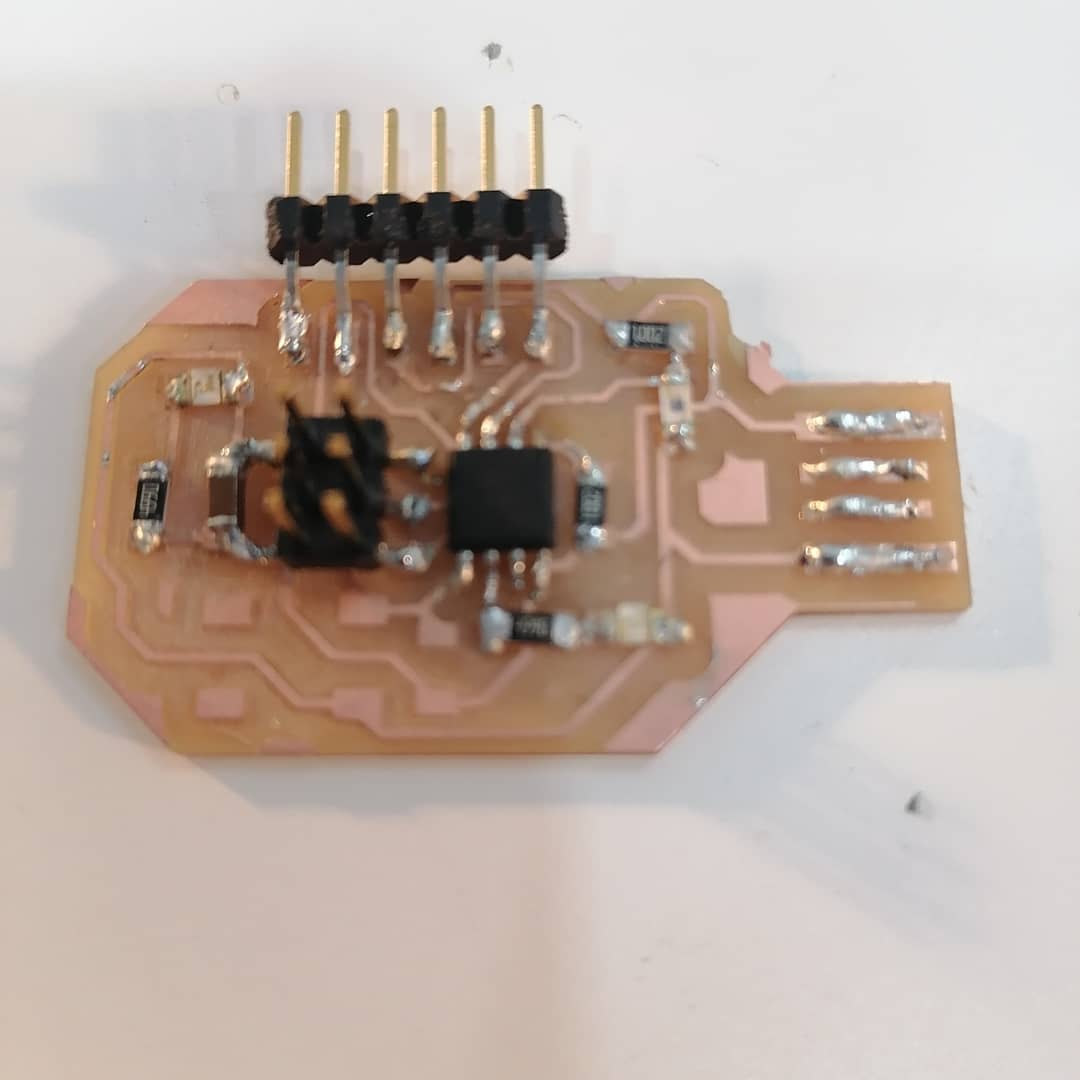
PCB soldering
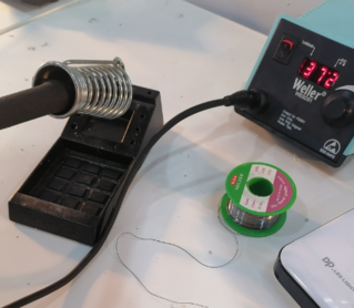
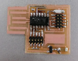
To solder the PCB componnet we need soldering iron, flux pen, led wire, tewwzers and Fume extractor fan.
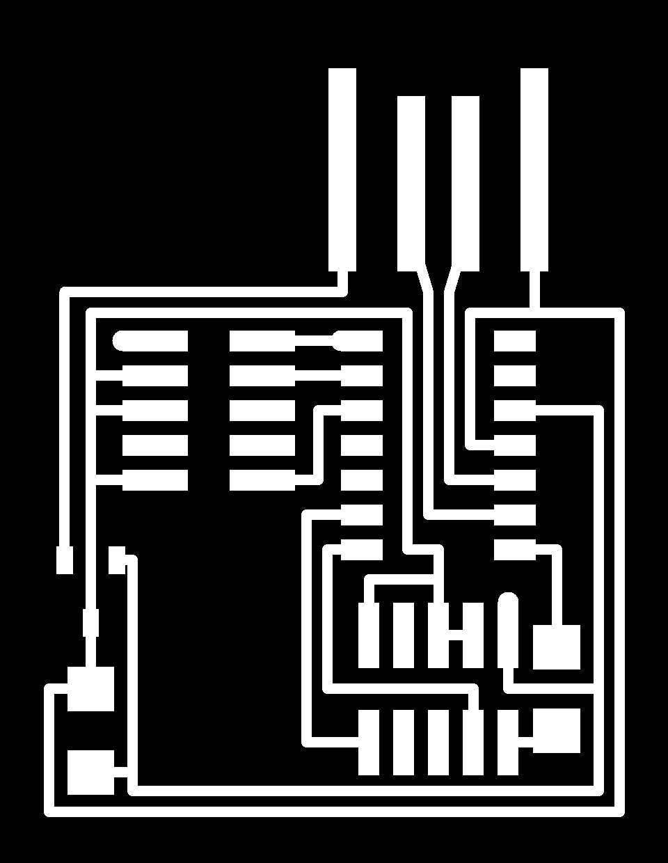
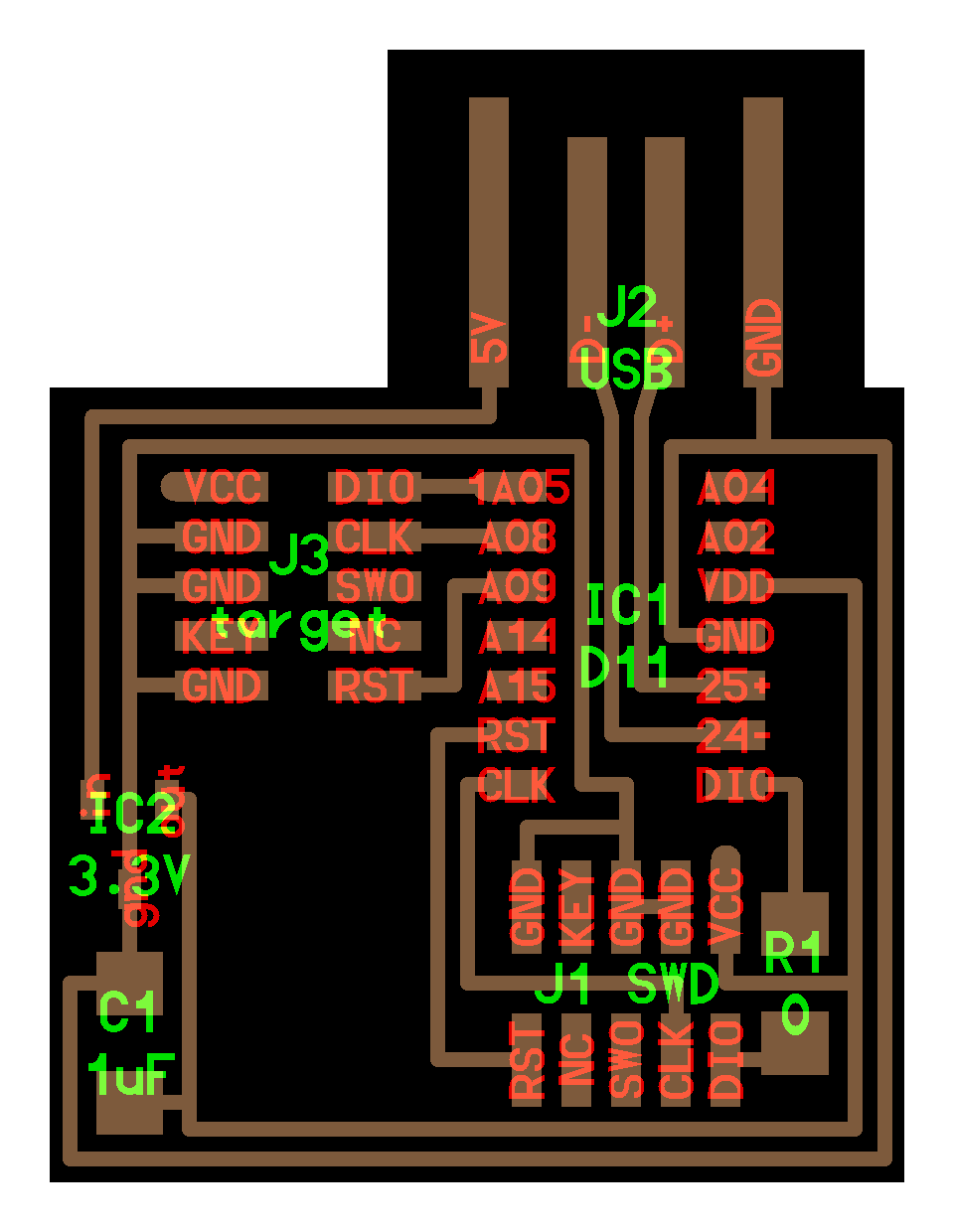
From the Circuit diagram we could now The circuit component, which are 0Ω resistance, 1µf capacitor, ATSAMD11C14A which is the microcontroller, 3.3v voltage regulator and two headers.
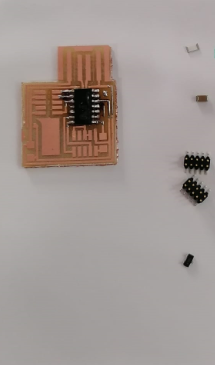
In order to start soldering first use the flux pen by moving it on the pleases where the circuit component must by placed it helps to stick them in the circuit board. After I was done with the flux pen, I place the SMD component in their places. Heat the soldering iron, add some soldering material to it and pass it through the pins or the terminals of the components. The result shown in the figure below
Programming
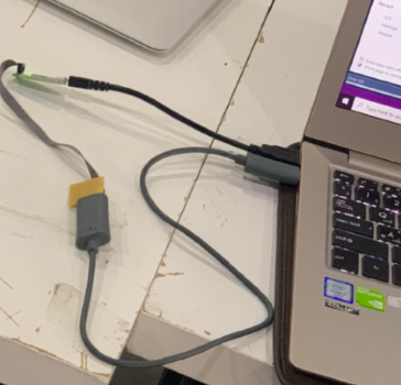
To check where is my PCB is working or not, I need to install the program in the microcontroller by a programmer that we made in the lab. To do this first I connect it with the J-LINK EDU Mini, then connect it to my PC. I use Atmel studio to communicate with the ATSAMD11 but before that I install J-Link tool because I am using the J-LINK cable.
You can see all the information about J-LINK EDU Minin here
After installing all the necessary tools, I open Atmel studio select tools << Device programming
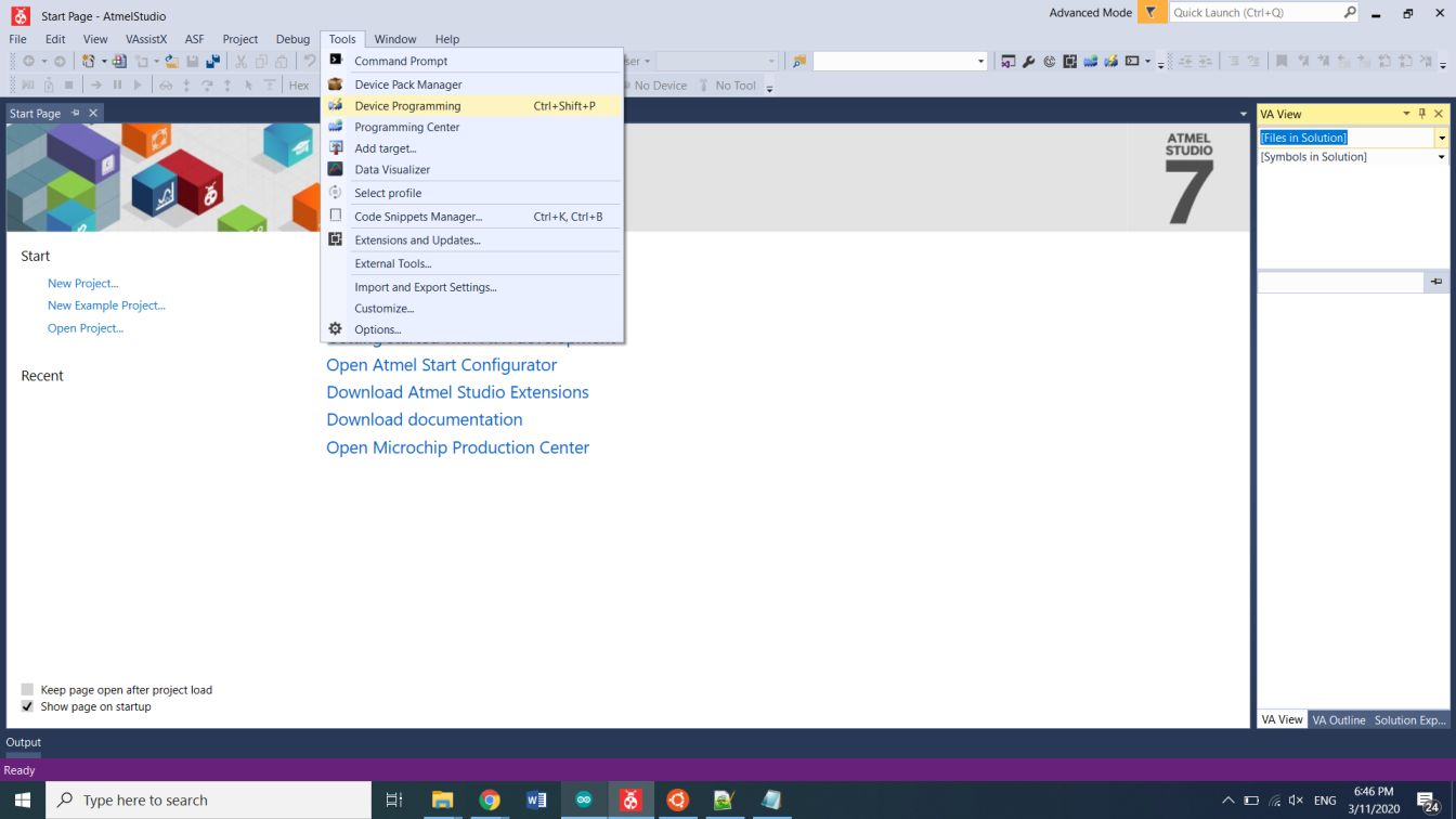
A new window will be open with the selected name -Device programming- I select the Tool “J-LINK”, Device “ATSAMD11C14A” and interface “SWD” then I click apply.
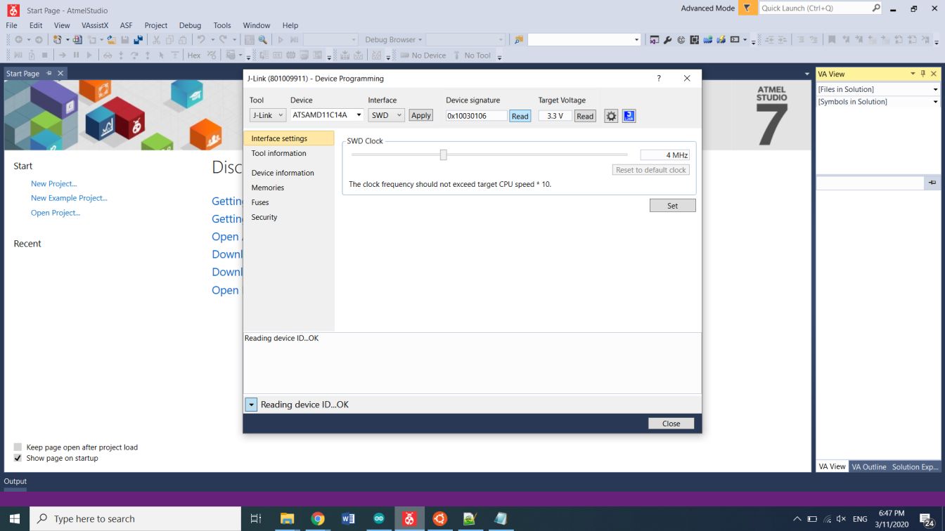
Download the binary file from fab academy, then from the same device programming window, go to memory << under Flash (16KB) brows to upload the binary file and then click program.
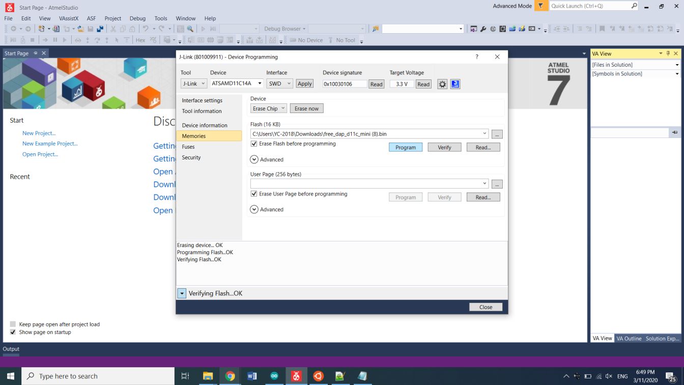
You can see the results from the white box in the picture above that erasing the device, programming flash and verifying flash are all done with no error.
Problems and Solution
One of the problems that I face in this assignment that I solder the microcontroller in the opposite direction so I de-solder it and re-solder it in the right direction.