Carvera making PCB
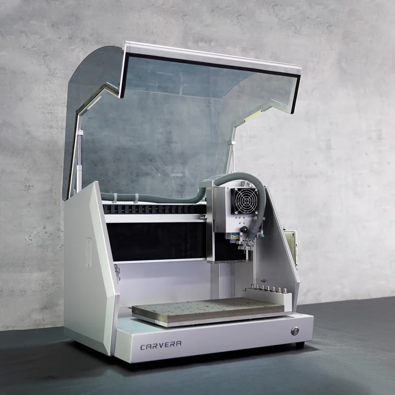 Carvera Desktop CNC Machine |
 |
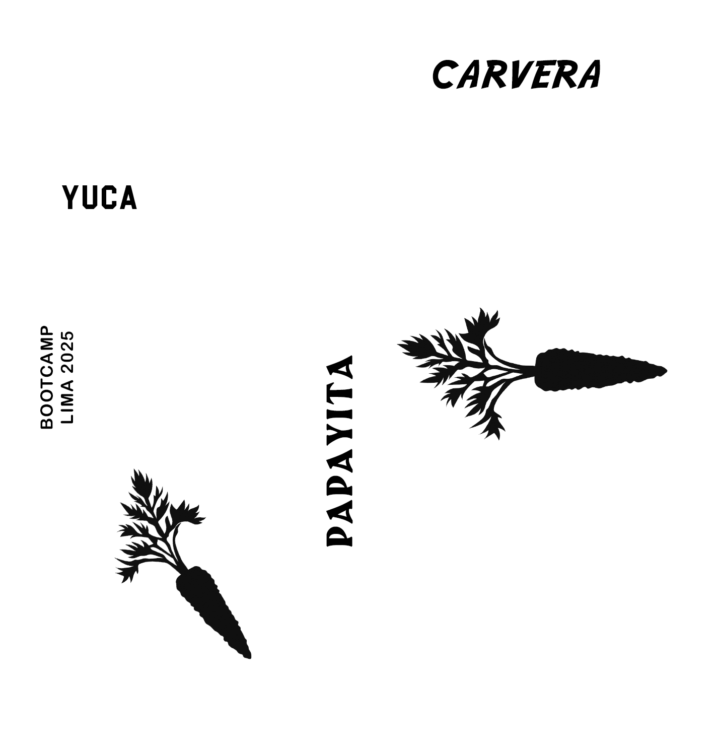
Team
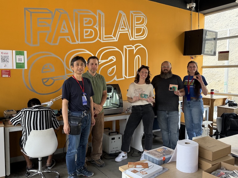
- Sedat Yalcin (Fab Lab Hisar Idealab, Istanbul, Turkey)
- Mark Blanc (ESAN, Lima, Peru)
- Nicole Stancampiano (PAST Innovation Fab Lab, Columbus, United States)
- Kelleigh Huey (PAST Innovation Fab Lab, Columbus, United States)
- Yuichi Tamiya (FabLab Kannai, Yokohama, Japan)
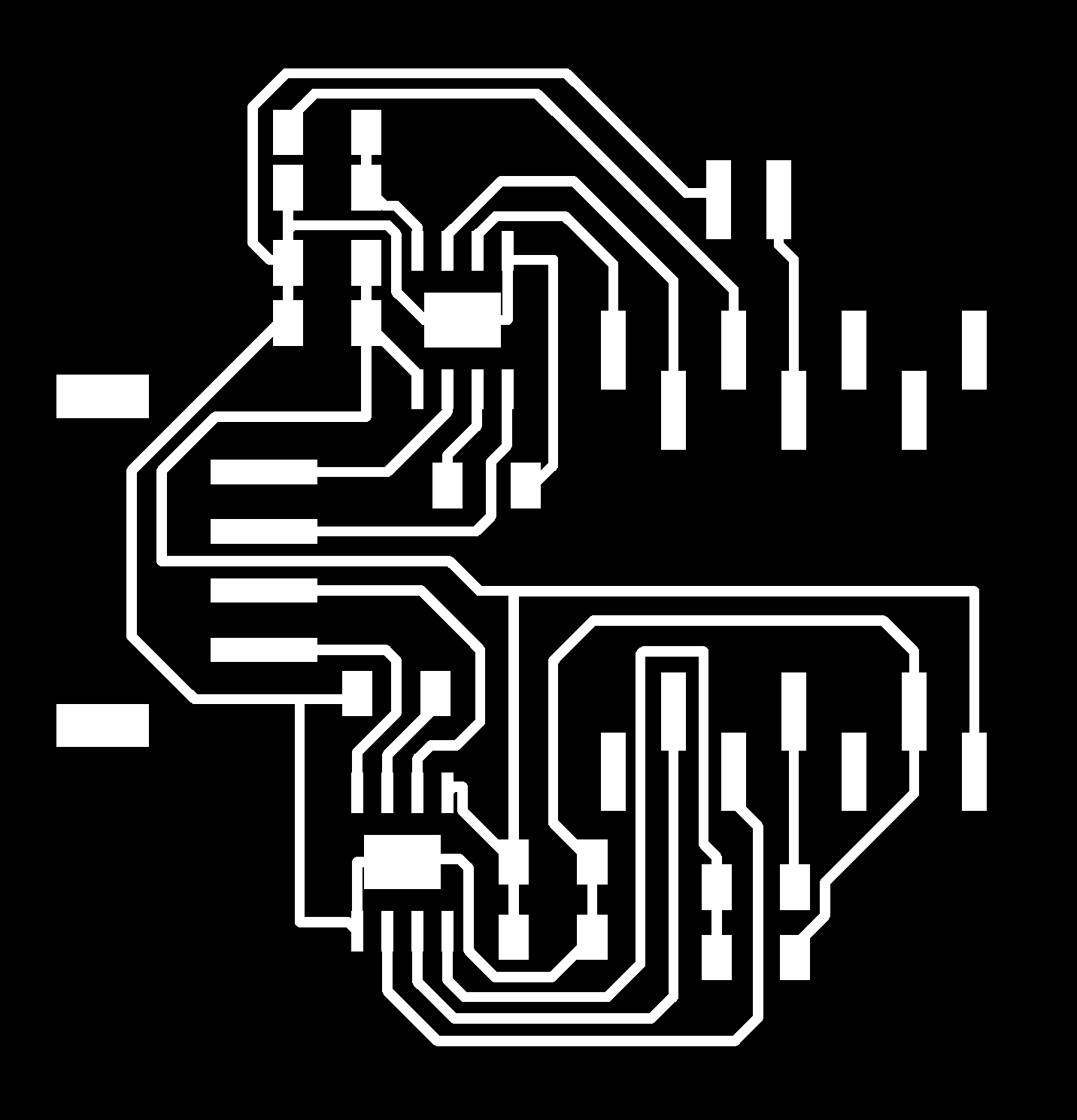
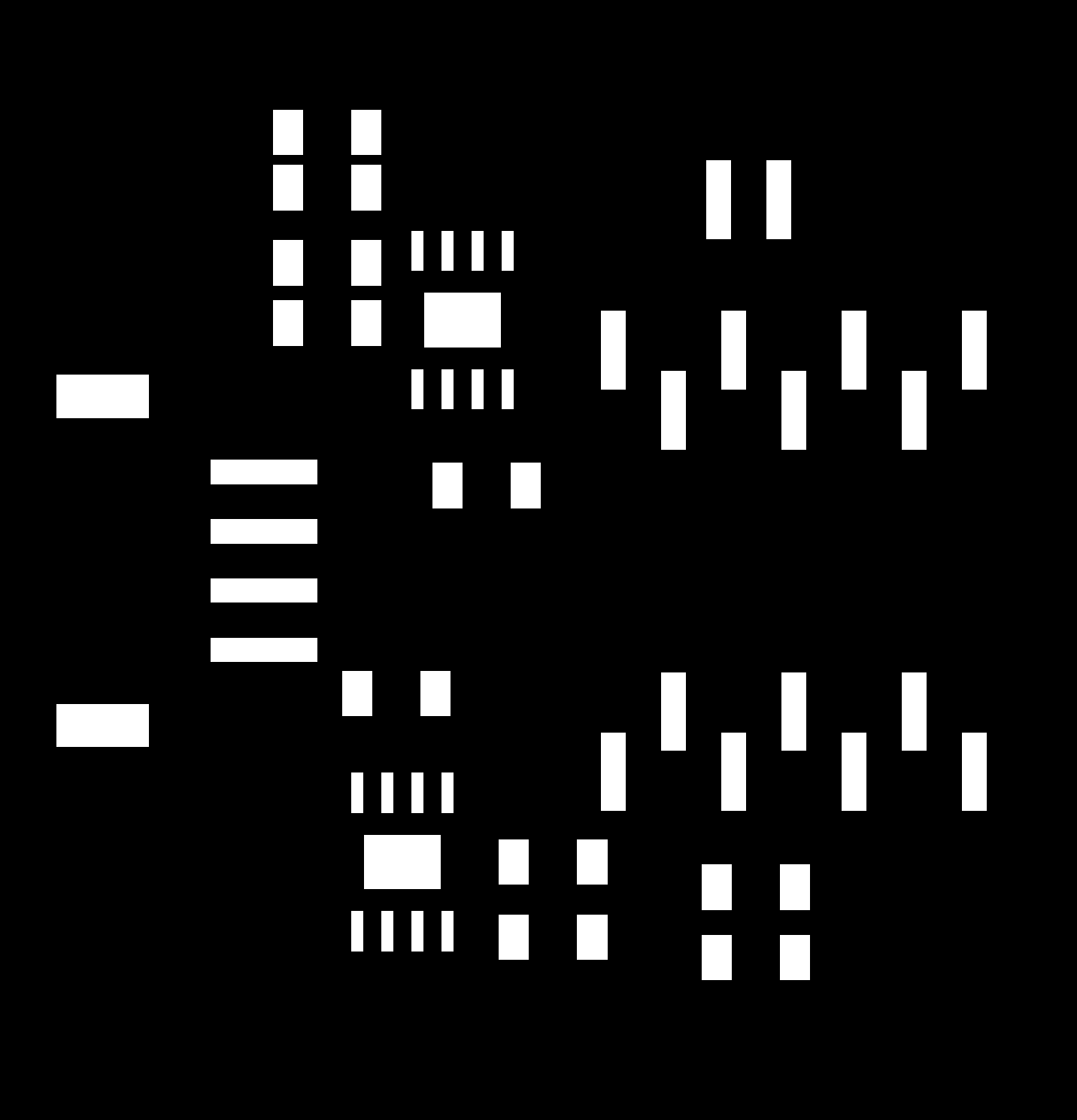
PCB design
Ref. Instructor bootcamp 2024 Leon
| Trace and Interior | Foot Print |
|---|---|
 |
 |
 |
PNG image size 45.47x 47.28mm, 800dpi Download Fusion360 Electronics file |
Preparation
Tool setting
- Tool 3: 0.8mm Corn Bit (1/32")
- Tool 4: Single Flute Bit 30_Deg (1/64")
- Tool 5: UV solder mask removal tool
Process
Ref. Carvera PCB tutorial
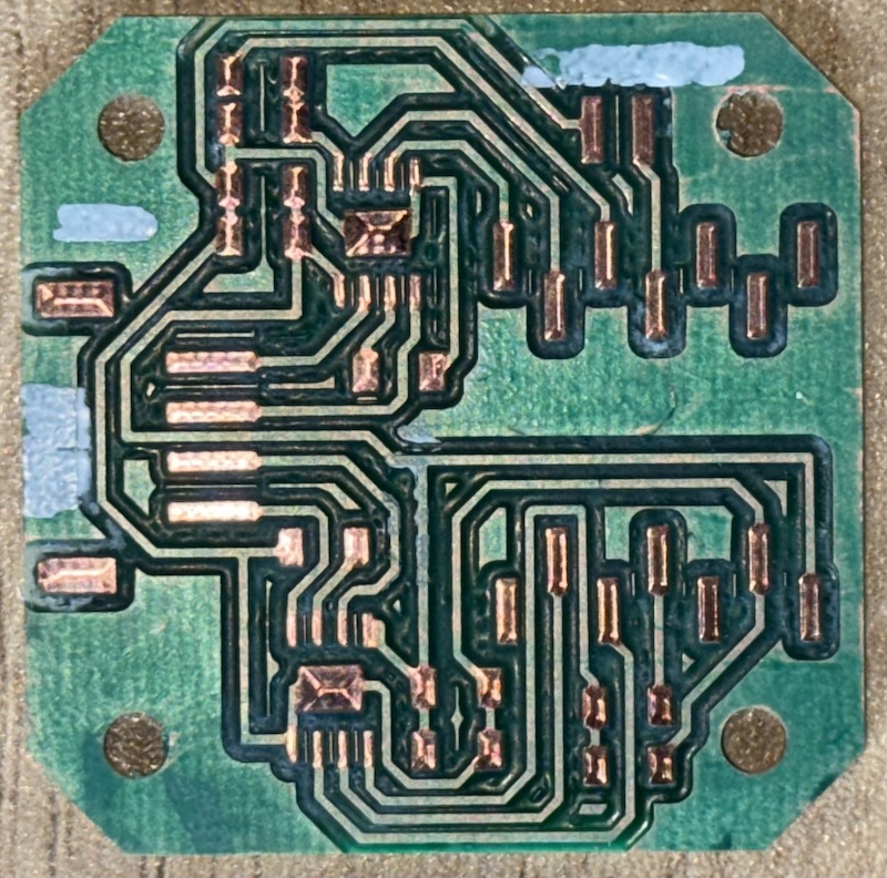
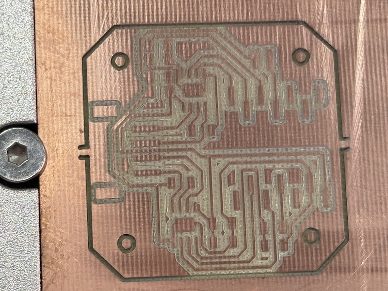
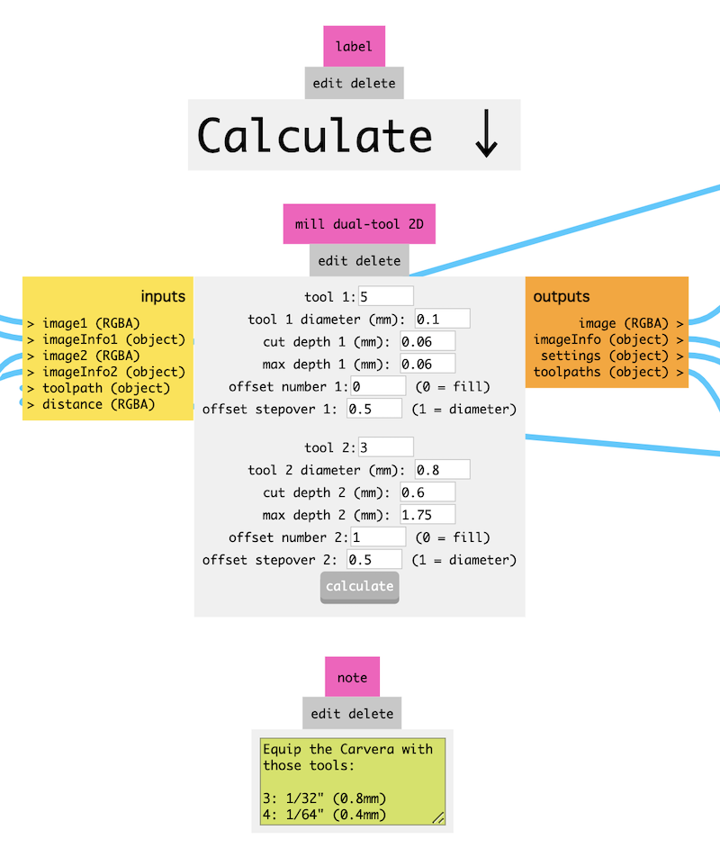
Process-1: Generate Toolpath(trace and interior)
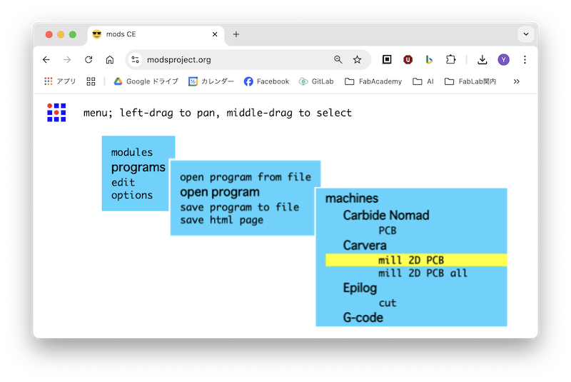
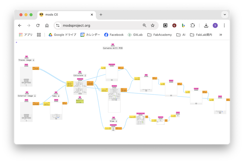
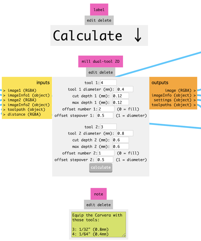
↑Click above image to enlarge "mill dual-tool 2D module" settings
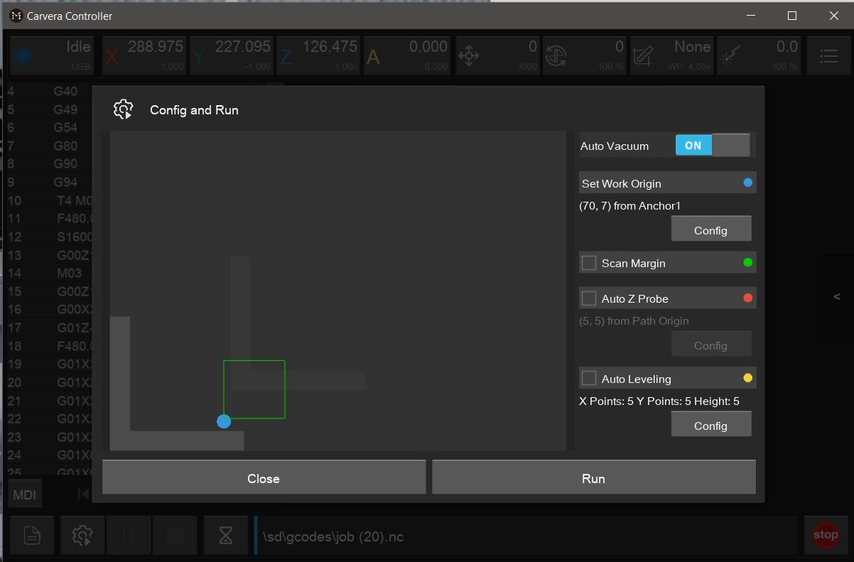
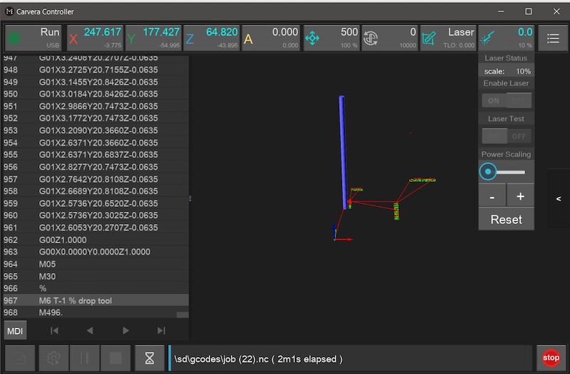
Process-2: Cavera Controller
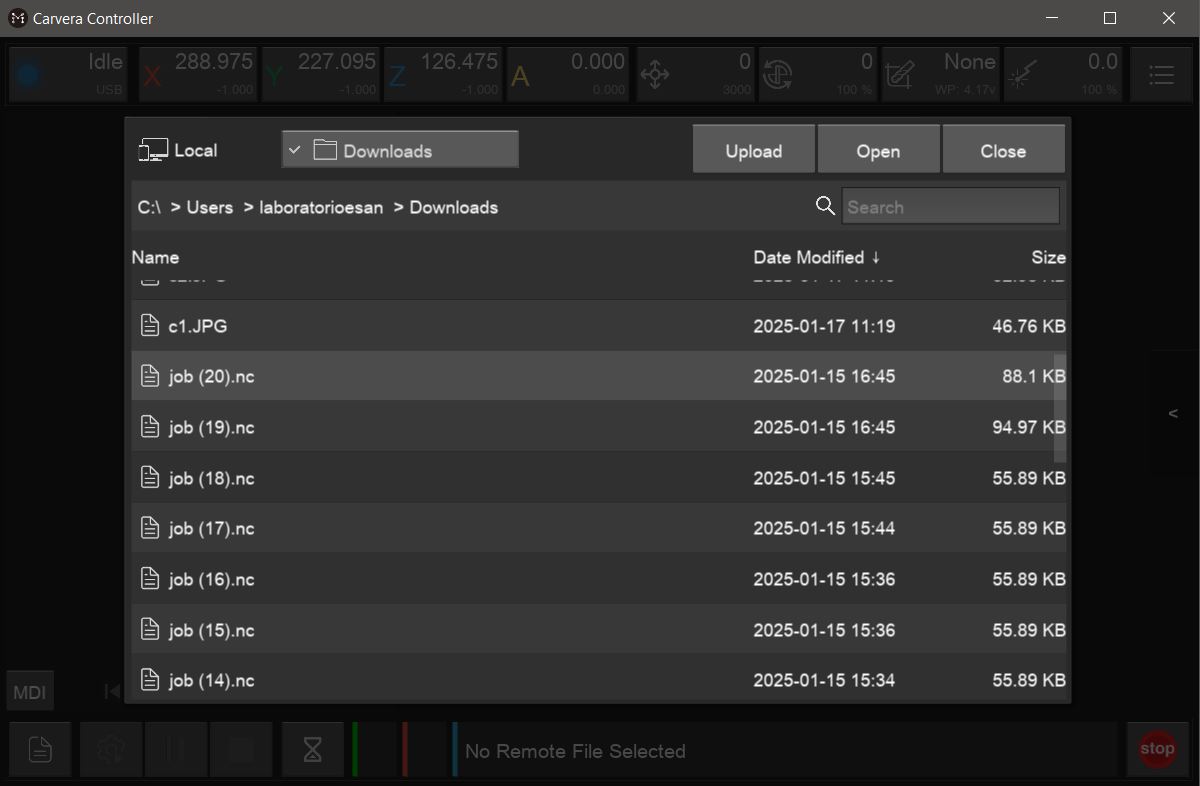
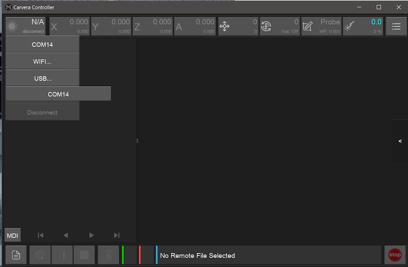 Connect USB |
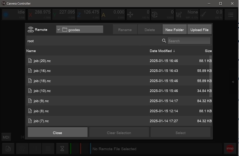 Go to Upload File |
 Serect .nc file |
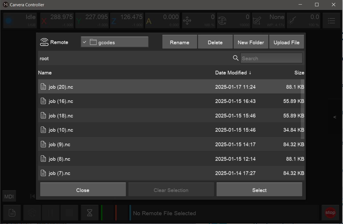 Click Select |
 path is appeared |
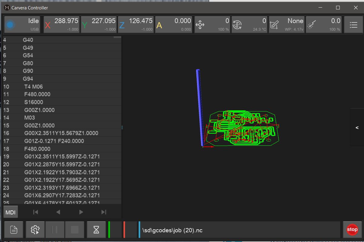
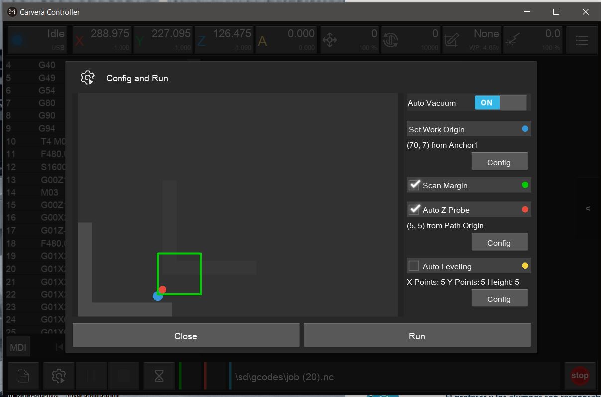 Set Work Origin and Run |
Note
Interior max cut depth is 0.6 mm. If milled too deep, the UV-ink remains uncured in deep milled gap
Process-3: Deburring
Use sanding tool/paper
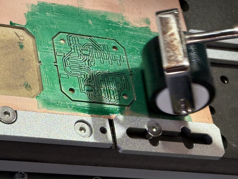
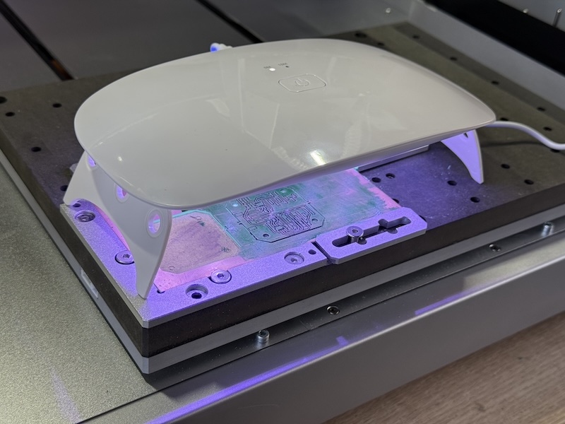
Process-4: Apply UV Curing Solder Mask Ink and Cure
Process-5: Toolpath(Foot Print)
Note
Invert Foot Print image
Tool 5: UV solder mask removal tool
↑Click above image to enlarge "mill dual-tool 2D module" settings
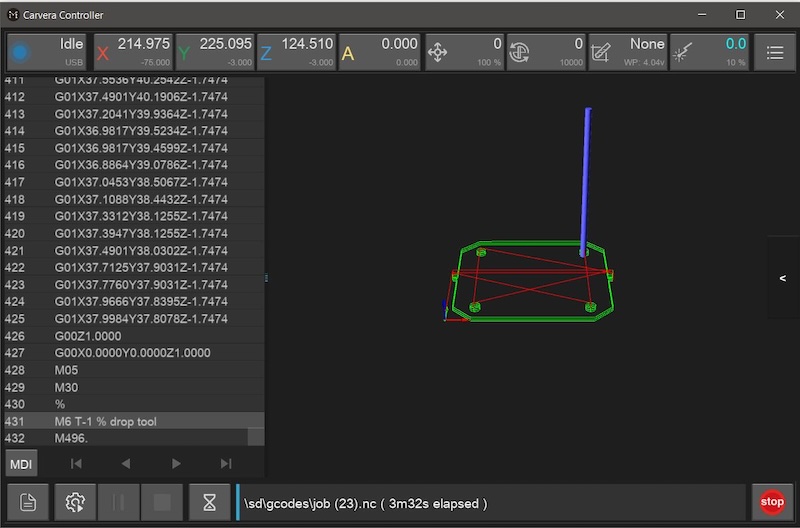
Process-6: Cavera Controller
Note
Scan Margin -> uncheck
Auto Leveling -> uncheck
Process-7: Apply UV Curing Solder Mask "White" Ink
Process-8: tool path
Note
offset number: 1
Process-9: laser engrave
Scale(Laser Power):10%
Process-10: Wipe
Note
don't use alcohol or it may remove some of the green layer
Process-11: Mill Interior
Mods -> Interior -> max cut depth: 1.7mm
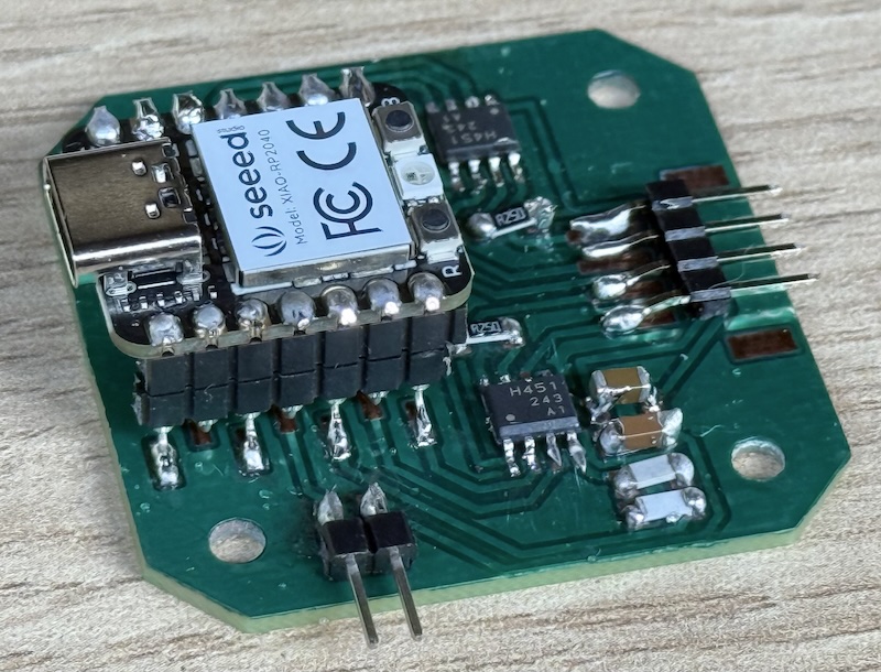
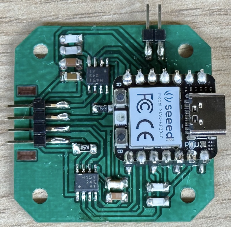
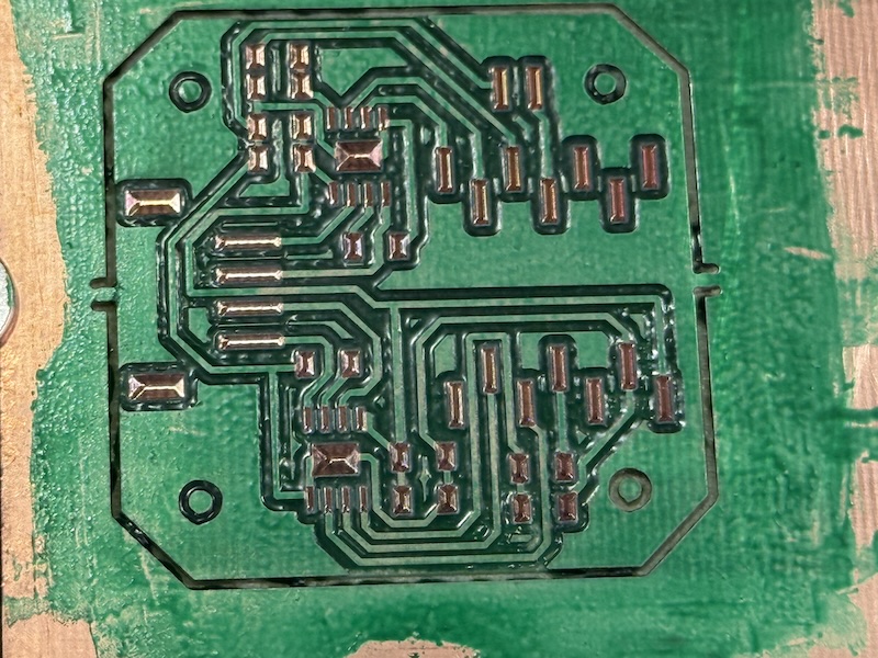
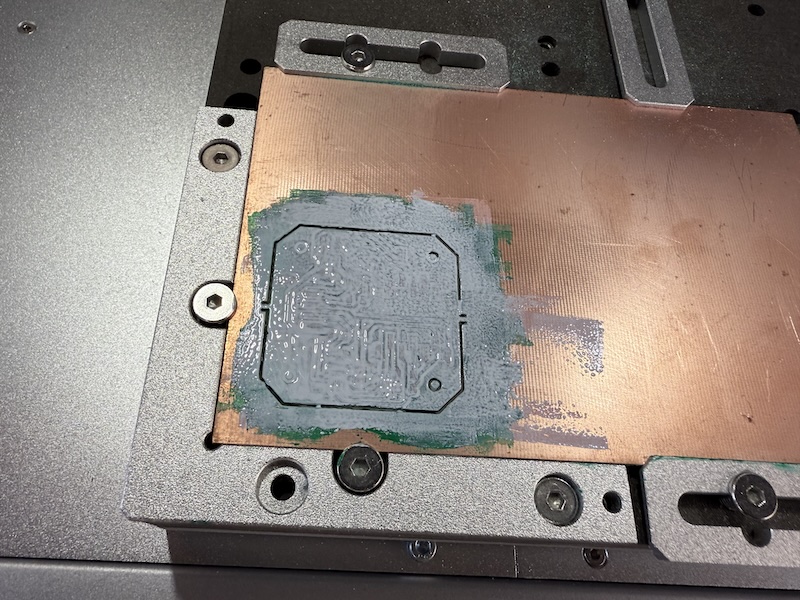
Final Result
Soldered PCB