8. Embedded Programming
This week assigment
group assignment:
- compare the performance and development workflows
for other architectures
Group project page
individual assignment:
- program your board to do something,
with as many different programming languages
and programming environments as possible
- read a microcontroller data sheet
Programming
Modify the board
Before programming, I discovered an important mistake.
Compared to last year’s instructor board diagram, I noticed that there was no button and LED wiring.
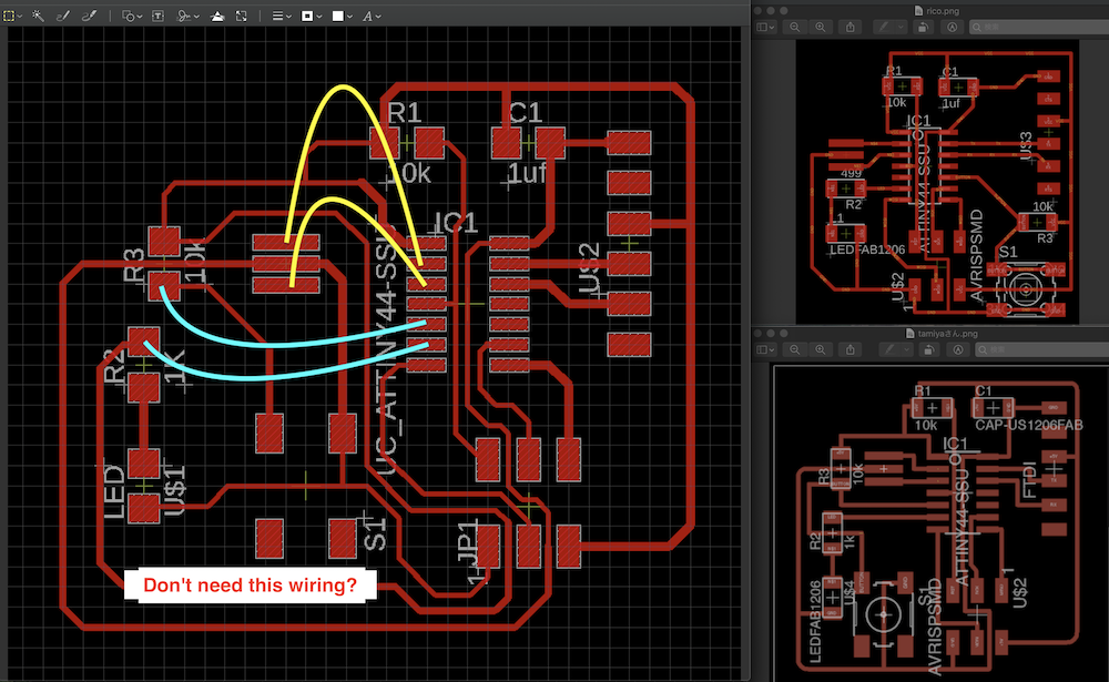
I investigated the cause with the advice of the instructor.
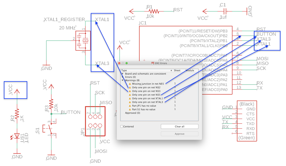
- What seems to be connected is not actually connected
When you do ERC, it comes out as a warning, - Net looks like BUTTON
- Net looks like XTAL1
-
Net looks like XTAL3
But actually each
N $ 2, N $ 3, N $ 5 and not connected -
LED is directly connected to VCC. Since it is not connected to the signal line, it can not be controlled from Attiny.
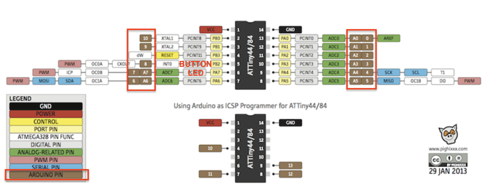
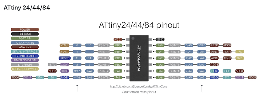
(How to fix by Asako_san) It is necessary to change VCC part to one of Attiny’s IO pins. Any pin can be connected as long as it is an IP pin, but preferably a pin that can use PWM (PB2 or PA7). Here is a beautifully rendered mapping of the ATTiny84 / ATTiny44 pins courtesy
I made a board diagram again. This time it worked.
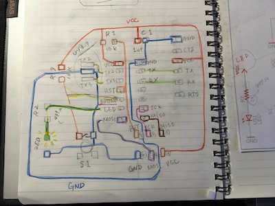
I tried to color the flow of VCC and GND by hand and finally found the flow of electricity.
I thought that hand-written analog work was also important.
The explanation by Riko’s diagram of the instructor was very easy to understand. Thank you.
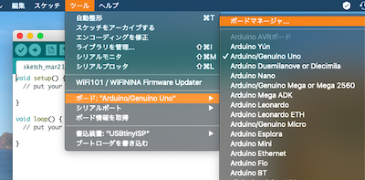
Arduino IDE
-
First I set Arduino IDE for ATtiny.
-
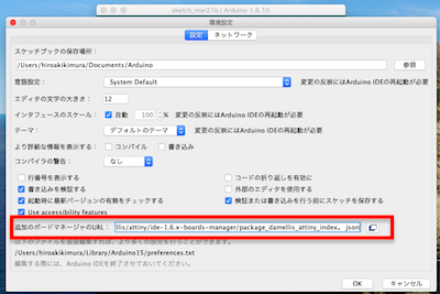
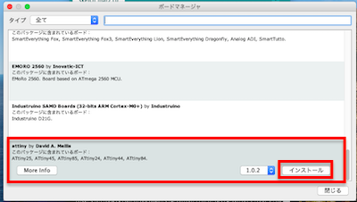
install the ATtiny support using the built-in boards manager.
Open preference then paste the following URL into the field and click OK https://raw.githubusercontent.com/damellis/attiny/ide-1.6.x-boards-manager/package_damellis_attiny_index.json
- install the ATtiny support using the built-in boards manager.
// constants won't change. They're used here to set pin numbers:
const int buttonPin = 2;     // the number of the pushbutton pin
const int ledPin =  13;      // the number of the LED pin

// variables will change:
int buttonState = 0;         // variable for reading the pushbutton status

void setup() {
  // initialize the LED pin as an output:
  pinMode(ledPin, OUTPUT);
  // initialize the pushbutton pin as an input:
  pinMode(buttonPin, INPUT);
}

void loop() {
  // read the state of the pushbutton value:
  buttonState = digitalRead(buttonPin);

  // check if the pushbutton is pressed. If it is, the buttonState is HIGH:
  if (buttonState == HIGH) {
    // turn LED on:
    digitalWrite(ledPin, HIGH);
  } else {
    // turn LED off:
    digitalWrite(ledPin, LOW);
  }
}
The default settings were as follows, so change them to actual numbers by pin mapping.
const int buttonPin = 2;     // the number of the pushbutton pin
const int ledPin =  13;      // the number of the LED pin
The button is connected to No.5 of ATTiny44 → Arduino pin number (brown) is No.8
The button is connected to No.6 of ATTiny44 → Arduino pin number (brown) is No.7
Change each.
const int buttonPin = 8;     // the number of the pushbutton pin
const int ledPin =  7;      // the number of the LED pin
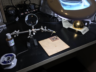
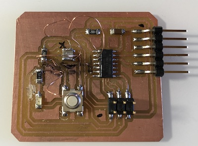
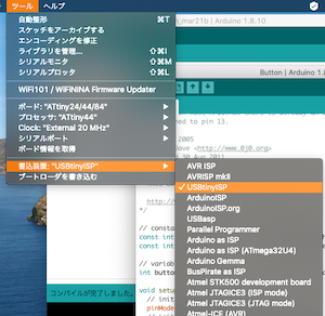
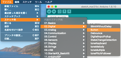
Write to microcomputer board
download-file: button.ino
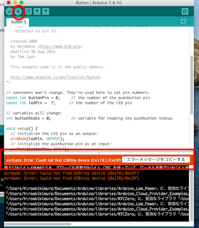
error
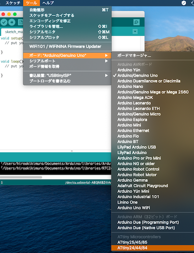
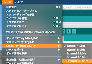
Since processor was ATtiny24, modified to ATtiny44.
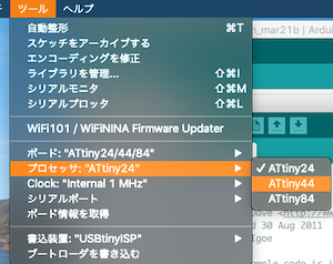
Clock corrected to 20 MHz
Write to microcomputer board
Microcomputer configuration
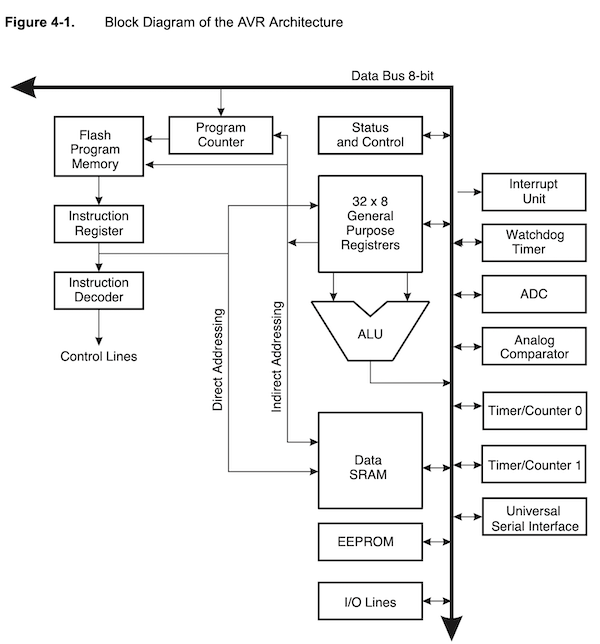
The microcomputer consists of I / O, CPU, ROM, RAM, and peripheral circuit components as shown in the figure.
By combining these parts,
The microcontroller operates as follows: “Accepts some input, performs certain processing, and outputs some signal.”
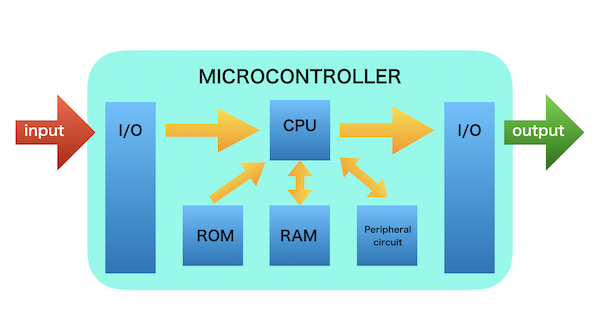
To explain the role of each part,
- I / O: A part that receives some input and outputs some signal.
- CPU: The part that performs certain processing.
- ROM: The part where the software that determines the processing content is stored.
- RAM: A part that stores temporary data such as processing results.
- Peripheral circuits: Circuits that enhance the functions of the microcomputer.
AVR data sheet
Read the AVR ATtiny44A datasheet and highlight some points of interest.
ATTiny is a series of low power microcontrollers among AVR microcontrollers manufactured by Atmel.
Since the operating voltage is low (1.8V ~), it can be easily operated even with dry batteries.
ATTiny microcomputer can write from Arduino.
Features
- High Performance, Low Power AVR® 8-bit Microcontroll er
- Endurance: 10,000 Write/Erase Cycles
- Data Retention: 20 years at 85°C / 100 years at 25°C
- Operating Voltage: – 1.8 – 5.5V
- Speed Grade: 0–20MHz@4.5–5.5V
- Low Power Consumption Active Mode: 210μAat1.8Vand1MHz
1. Pin Configurations
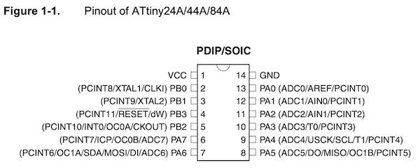
Pin Descriptions
- VCC: Supply voltage.+
- GND: Ground.−
- Port B (PB3:PB0): Port B is a 4-bit bi-directional I/O port with internal pull-up resistors (selected for each bit).
- RESET: Reset input.
- Port A (PA7:PA0): Port A is a 8-bit bi-directional I/O port with internal pull-up resistors (selected for each bit).
2. Overview
- ATtiny24A/44A/84A are low-power CMOS 8-bit microcontrollers based on the AVR enhanced RISC architecture.
- The AVR core combines a rich instruction set with 32 general purpose working registers. All 32 registers are directly connected to the Arithmetic Logic Unit (ALU), allowing two independent registers to be accessed in one single instruction executed in one clock cycle.
3. General Information
- Typical values contained in this datasheet are based on simulations and characterization of other AVR microcontrollers manufactured on the same process technology. Min and Max values will be available after the device has been characterized.
4. CPU Core
Architectural Overview
- For maximum efficiency and parallel processing, the AVR uses a Harvard architecture that separates memory and bus for program and data.
- The program memory is a flash memory that can be mounted and rewritten.
- The high-speed register file contains 32 8-bit general-purpose registers accessed in one clock cycle.
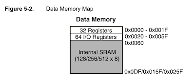
5. Memories
- The AVR architecture has two main memory spaces, the Data memory and the Program memory space. In addition, the ATtiny24A/44A/84A features an EEPROM Memory for data storage. All three memory spaces are linear and regular.
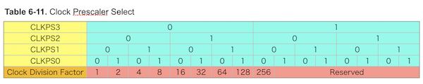
6. Clock System
The sequential circuit operates in synchronization with the rising (the signal changes from L to H) or falling (the signal changes from H to L) of the clock signal (clk). Since the microcomputer is also composed of sequential circuits, an external oscillator circuit is connected to supply the clock. The clock input from outside the microcomputer is called “external clock signal”.
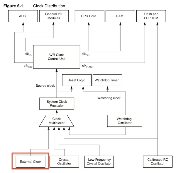
The unit is expressed in frequency [Hz].
If this clock is faster, instructions can be executed faster. The CPU executes instructions in order according to this clock.

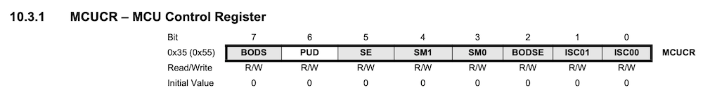
- Bit 7 – CLKPCE: Clock Prescaler Change Enable
The CLKPCE bit must be written to logic one to enable change of the CLKPS bits. The CLKPCE bit is only updated when the other bits in CLKPR are simultaniosly written to zero. CLKPCE is cleared by hardware four cycles after it is written or when the CLKPS bits are written. Rewriting the CLKPCE bit within this time-out period does neither extend the time-out period, nor clear the CLKPCE bit.
7. Power Management and Sleep Modes
The high performance and industry leading code efficiency makes the AVR microcontrollers an ideal choise for low power applications. In addition, sleep modes enable the application to shut down unused modules in the MCU, thereby saving power. The AVR provides various sleep modes allowing the user to tailor the power consumption to the application’s requirements.
8. System Control and Reset
During reset, all I/O Registers are set to their initial values, and the program starts execution from the Reset Vector. The instruction placed at the Reset Vector must be a RJMP – Relative Jump – instruction to the reset handling routine. If the program never enables an interrupt source, the Interrupt Vectors are not used, and regular program code can be placed at these locations.
The I/O ports of the AVR are immediately reset to their initial state when a reset source goes active. This does not require any clock source to be running.
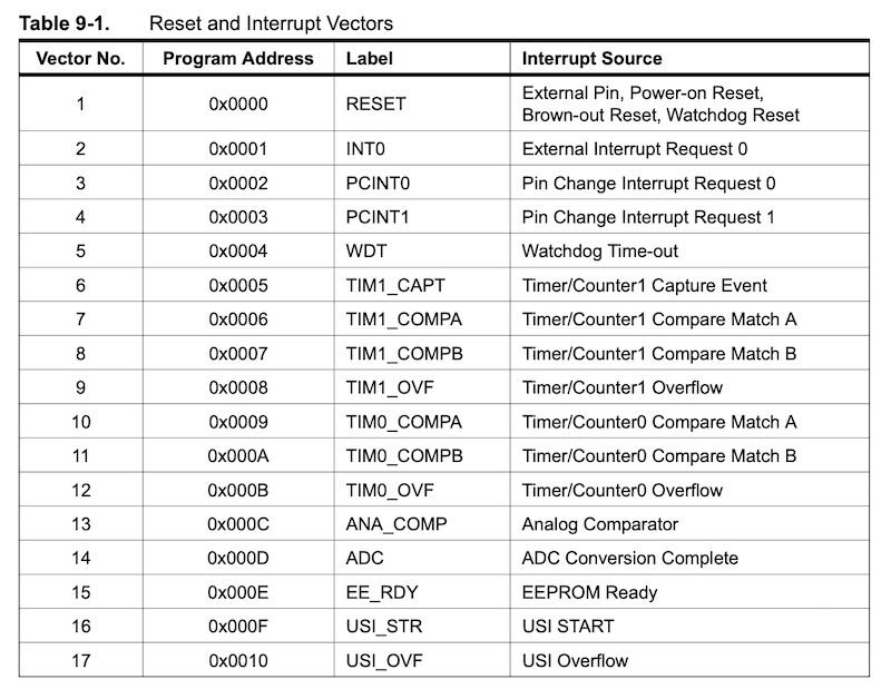
9. Interrupts
The priority of interrupts is as follows. Reset is the 1st priority, and the second is External interrupt INT0. PCINT0 and PCINT1 are Pin change interrupt. It is able to use all PA/PB port pins as interrupt PCINTxx.
I reffered the code example of intereupt in the hello.echo board c.
The flow is three steps.
- First enable the pin change interrupt by GIMSK PCIE0 bit.
- Define the interrupt pin with PCMSK0 or PCMSK1.
- After that enable the interrupt by sei().
#define serial_interrupt (1 << PCIE0)
#define serial_interrupt_pin (1 << PCINT0)


// set up pin change interrupt on input pin
   //
   set(GIMSK, serial_interrupt);
   set (PCMSK0, serial_interrupt_pin);
   sei();
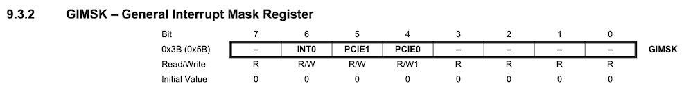
• Bit 4 – PCIE0: Pin Change Interrupt Enable 0
When the PCIE0 bit is set (one) and the I-bit in the Status Register (SREG) is set (one), pin change interrupt 0 is enabled. Any change on any enabled PCINT[7:0] pin will cause an inter- rupt. The corresponding interrupt of Pin Change Interrupt Request is executed from the PCI0 Interrupt Vector. PCINT[7:0] pins are enabled individually by the PCMSK0 Register.
• Bits 7:0 – PCINT[7:0]: Pin Change Enable Mask 7:0
Each PCINT[7:0] bit selects whether pin change interrupt is enabled on the corresponding I/O pin. If PCINT[7:0] is set and the PCIE0 bit in GIMSK is set, pin change interrupt is enabled on the corresponding I/O pin. If PCINT[7:0] is cleared, pin change interrupt on the corresponding I/O pin is disabled.
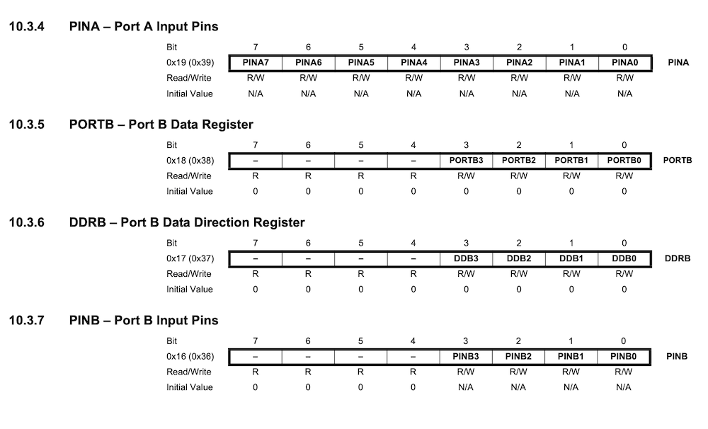
10. I/O Ports
Configuring the Pin(p.54)
Each port pin consists of three register bits: DDxn, PORTxn, and PINxn. As shown in “Register Description” on page 66, the DDxn bits are accessed at the DDRx I/O address, the PORTxn bits at the PORTx I/O address, and the PINxn bits at the PINx I/O address.
The DDxn bit in the DDRx Register selects the direction of this pin. If DDxn is written logic one, Pxn is configured as an output pin. If DDxn is written logic zero, Pxn is configured as an input pin.
If PORTxn is written logic one when the pin is configured as an input pin, the pull-up resistor is activated. To switch the pull-up resistor off, PORTxn has to be written logic zero or the pin has to be configured as an output pin. The port pins are tri-stated when reset condition becomes active, even if no clocks are running.
If PORTxn is written logic one when the pin is configured as an output pin, the port pin is driven high (one). If PORTxn is written logic zero when the pin is configured as an output pin, the port pin is driven low (zero).
Toggling the Pin(p.55)
Writing a logic one to PINxn toggles the value of PORTxn, independent on the value of DDRxn. Note that the SBI instruction can be used to toggle one single bit in a port.
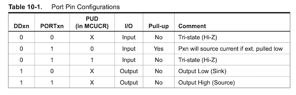
Register Description(p.66)
• Bit 6 – PUD: Pull-up Disable
When this bit is written to one, the pull-ups in the I/O ports are disabled even if the DDxn and PORTxn Registers are configured to enable the pull-ups ({DDxn, PORTxn} = 0b01). See “Con- figuring the Pin” on page 54 for more details about this feature.
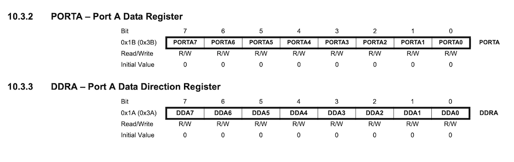
Port A is a 8-bit bi-directional I/O port and Port B is 4-bit. Internal pull-up exists for each port, and it is selectable. Port A has alternate functions such as ADC, timer/counter,SPI and pin change interrupt. Port B also has special functions such as Crystal Oscillator I/O, Reset,and pin change interrupt.
I reffered the code example of port initialization in the hello.echo board c.
#define serial_port PORTA
#define serial_direction DDRA
#define serial_pin_out(1 << PA1)

//出力ピンを初期化
//
  set(serial_port、serial_pin_out);
  output(serial_direction、serial_pin_out);
//
To initialize an output pin, set the direction with DDRA, then set the data to Data register.
As for input port, the initialization is not necessary, because the initial direction of port is input. To read the input port, we have to use PINx instead of PORTx.