Connecting 5V and 3V3
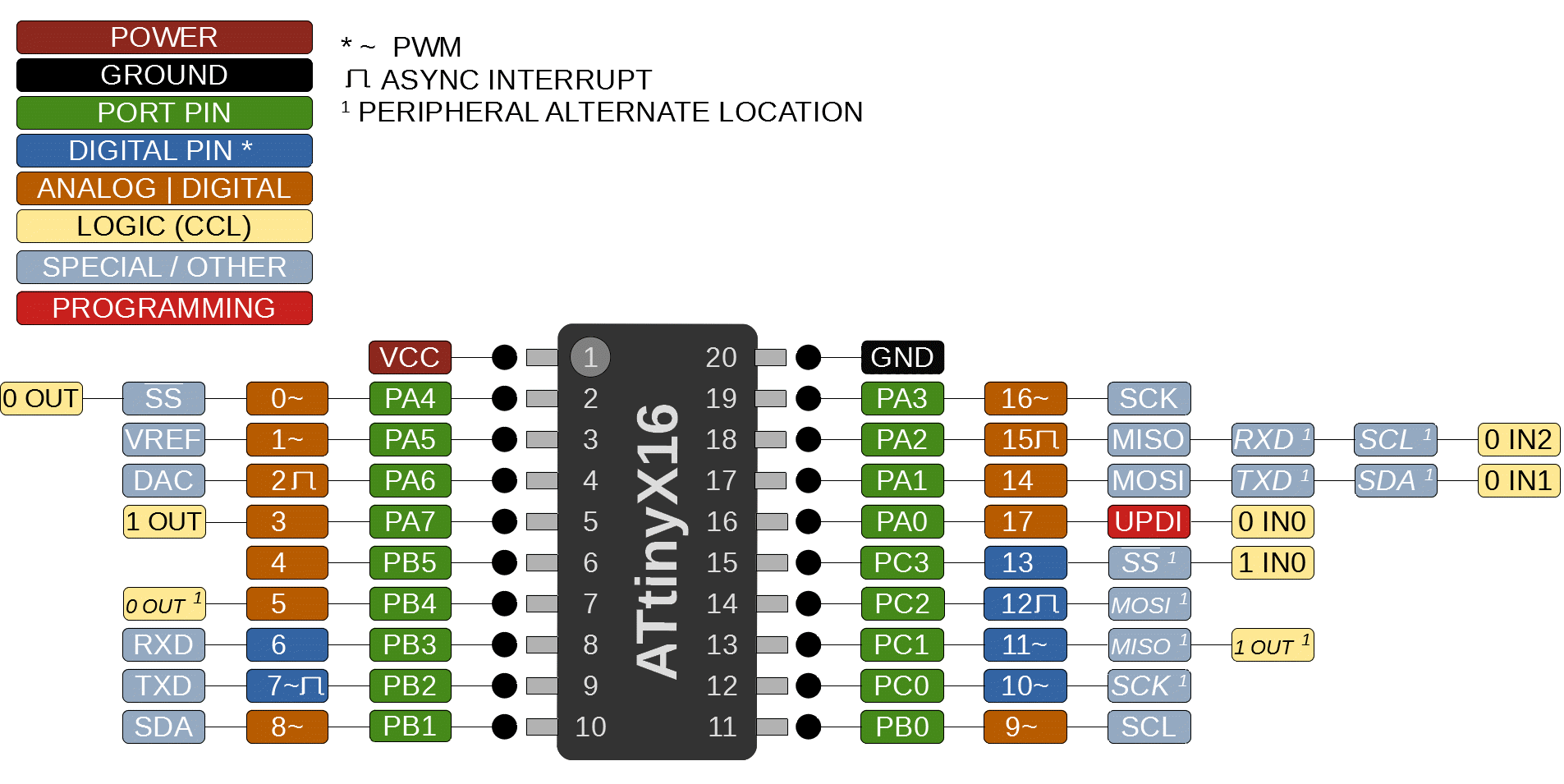
ATtiny3216
| Voltage - Supply (Vcc/Vdd) | 1.8V ~ 5.5V |
ref. digikey
ATtiny3216 can work with both 5V and 3.3V supply.
When VCC is 3.3V, all signals from this board will be 3.3V.
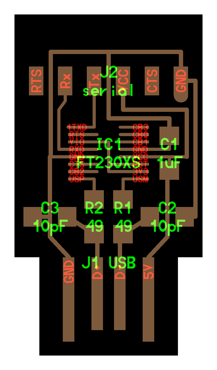
FT230XS
| Class USB-serial | Schematic Symbol |
|---|---|
 |
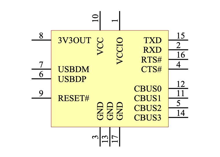 |
| Pin No. | Name | Type | Description |
|---|---|---|---|
| 10 | VCC | POWER Input | 5 V (or 3V3) supply to IC |
| 1 | VCCIO | POWER Input | 1V8 - 3V3 supply for the IO cells |
| 8 | 3V3OUT | POWER Output | 3V3 output at 50mA. May be used to power VCCIO.When VCC is 3V3; pin 8 |
ref. datasheet
In Class USB-serial board,
-
FT230XS’s VCC is connected 5V from USB and VCC of J2 serial. This means the power supplied from this FTDI board to your boards is 5V.
If you need to supply 3.3V to your board, we need 3.3V regulator externally before connecting VCC of your IC. -
VIO is connected 3V3. FT230XS is working with 1.8V, but IO voltage is set to 3.3V. This means Tx signal from FT230XS is regulated to 3.3V from 1.8V before send, Rx signal from other 5V IC will regulated to 3.3V internally in FT230XS chip.
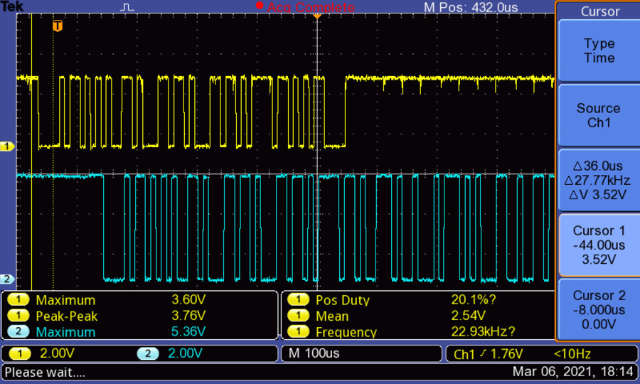
This is the Oscilloscope result.
- Signal 1 (Yellow) is from Tx of FTDI board. This shows Yellow is 3.3V range.
- Signal 2 (Blue) is from Rx of 3216 board supplied 5V VCC. This shows Blue is 5V range.
Connecting TFT module(3.3V), 3216(working with 3.3V) and class FTDI board(5V)
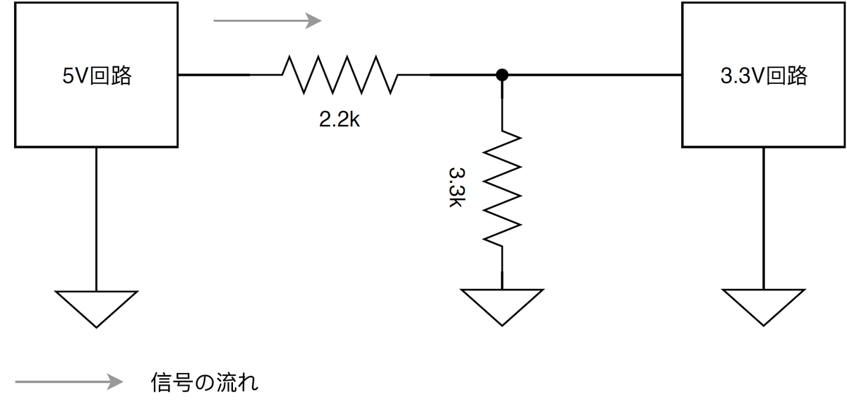
Voltage Devider Registers
In this tips, because Arduino UNO worked with 5V and TFT modules works with 3.3V, 2.2k and 3.3k Ohm registers were used as Voltage Divider registers.
Logic Level Converter
If Logic Level Converter is used instead of registers, Schematic will be simple.
3.3V regulator
On the other hand, if the IC working with 3.3V rather than 5V can be used, no need to think about Voltage difference. To do this, only a 3.3V regulator between 5V from FTDI and VCC to IC is needed to install.
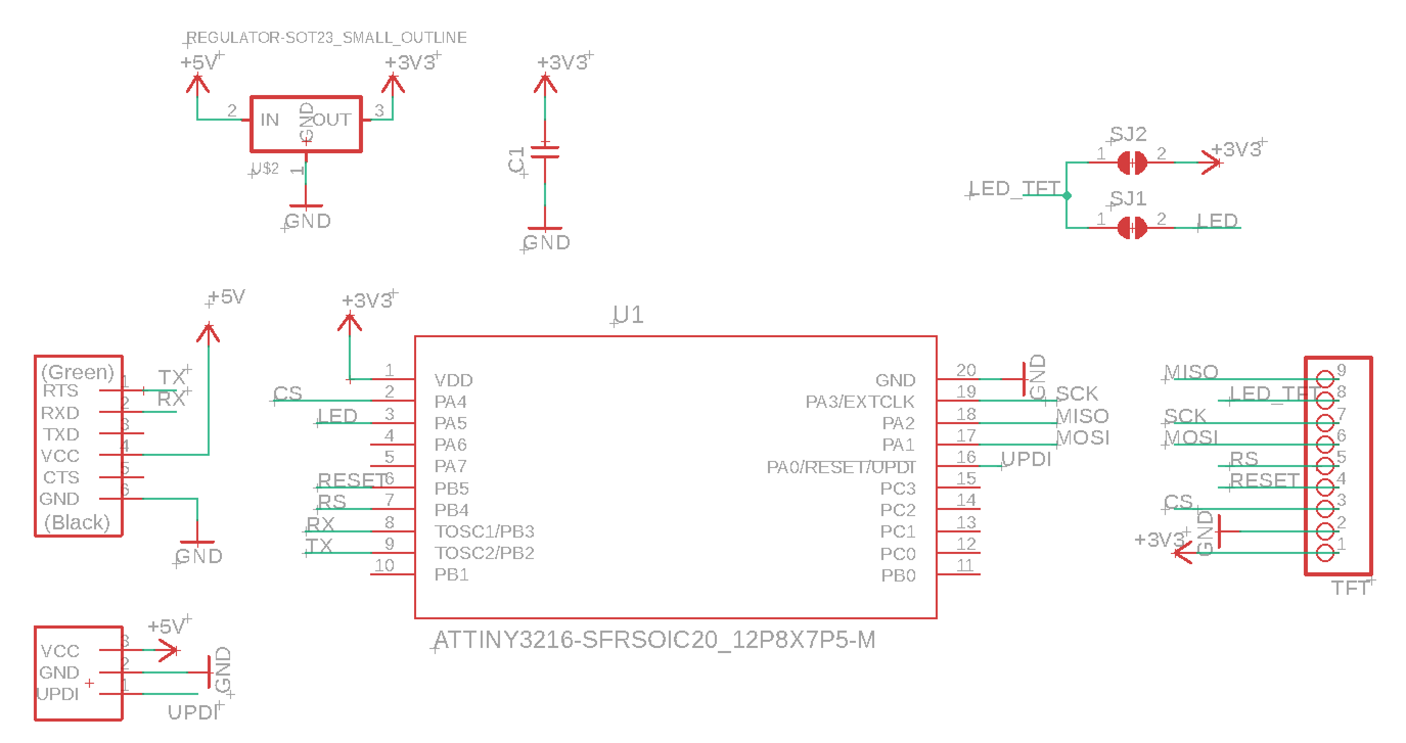
| PinNo | Printed on board | detail | SPI | my pin | |
|---|---|---|---|---|---|
| 9 | SDO/MISO | SerialDataOut/MasterInSlaveOut | yes | 12 /PA2 | |
| 8 | LED | BackLightLED | - | 1 /PA5 or 3.3V_reg_out | |
| 7 | SCK | Clock | yes | 16 /defined by system | |
| 6 | SDI/MOSI | SerialDstaIn/MasterOutSlaveIn | yes | 14 /defined by system | |
| 5 | DC/RS | DataCommand | - | 5 /PB4 | |
| 4 | RESET | - | 4 /PB5 | ||
| 3 | CS | ChipSelect | yes | 0 /PA4 | |
| 2 | GND | yes | GND | ||
| 1 | VCC | 5V/3.3V | 5V -> J1 Off(use_regulator) | 3.3V -> J1 Bridge(no_regulator) | 3.3V_reg_out |
Sample program
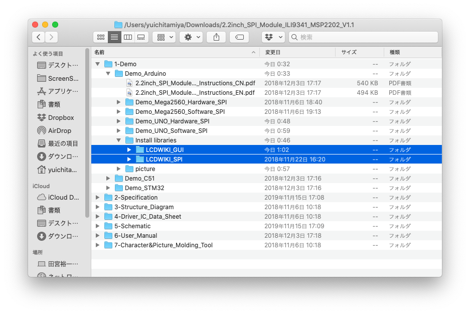
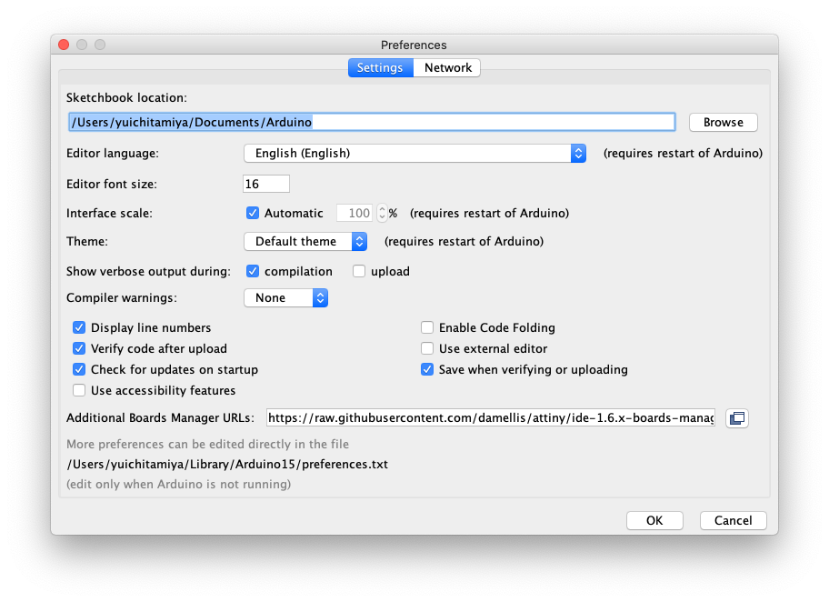
Copy these two dependent_libraly (LCDWIKI_GUI,LCDWIKI_SPI) to ArduinoIDE sketchbook location folder
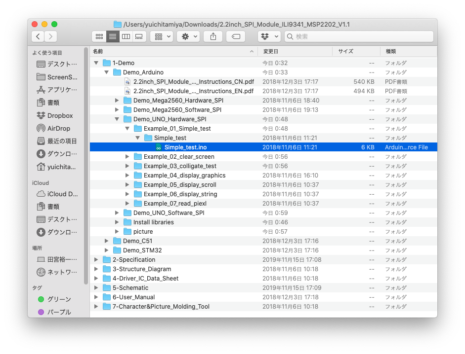
Open Simple_test.ino
1 2 3 4 5 6 7 8 9 10 11 12 13 14 15 16 17 18 19 20 21 22 23 24 25 26 27 28 29 30 31 32 33 34 35 36 37 38 39 40 41 42 43 44 45 46 47 48 49 50 51 52 53 54 55 56 57 58 59 60 61 62 63 64 65 66 67 68 69 70 71 72 73 74 75 76 77 78 79 80 81 82 83 84 85 86 87 88 89 90 91 92 93 94 95 96 97 98 99 100 101 102 103 104 105 106 107 108 109 110 111 112 113 114 115 116 117 118 119 120 121 122 123 124 125 126 127 128 129 130 131 132 133 134 135 136 137 138 139 140 141 142 143 144 145 146 147 148 149 150 151 152 153 154 155 156 157 158 159 160 161 162 163 164 165 166 167 168 169 170 171 172 173 174 175 176 177 178 179 180 181 182 183 184 185 186 187 188 189 190 191 192 193 194 195 196 197 198 199 200 201 202 203 204 205 206 207 208 209 210 211 212 213 214 215 216 217 218 219 220 221 222 223 224 225 226 227 228 229 230 231 232 233 234 235 236 237 238 239 240 241 242 243 244 245 246 247 248 249 250 251 252 | |