This week's assignment is to test the operation of a circuit board (in-group) and to design a hello-world board with additional buttons and LEDs (individual).
* All RML and original editable KiCad files can be downloaded here.
* To keep the momentum of the 4th week, I continued to consolidate a set of electronics design rules.
* This week's group assignment is to troubleshoot a circuit board using a multimeter.
* Besides, we are required to individually design our first PCBs and fabricate them.
Understanding EDA
This week's content was a bit easier for me to digest since I read about the basic components during the 4th week. This week, I want to learn about the principles of designing a functional circuit. Allow me to go through a very long note without any images attached, or go straight to the assignments below.
Electronic design automation (EDA) is a type of software used to design and simulate electronic systems such as ICs and PCBs. An EDA usually must be able to help us create schematics, generate Netlists, create PCB layouts (including routed traces and footprints), and generate Gerber files. I was thinking about sticking to the Autodesk family by using their EDA software Eagle. However, there were some reasons I went ahead with KiCad: it is free and open-source, and our instructor Oscar provided us with a very throughout tutorial regarding design steps using KiCad here.
EDA design flows
We indeed need to go through a bunch of EDA features to accomplish the design of an IC or a PCB. Some crucial steps:
- Schematic capture: the very first step of the actual design of an electronic circuit. Besides basic drawing and visualization capabilities, schematic editors typically provide the capabilities of hierarchical design as well as capturing electrical properties and other attributes of components, wires, nets, and pins.
- Placement: assign locations for circuit components (and footprints) within a netlist such that they fit within the available space and the router can make all of the necessary connections between them. A placement with good routability and density is a good placement. An inferior placement will not only affect the performance but might also make it non-manufacturable. The placement optimization objectives typically include minimize wire-length and avoid congestions.
- Routing: connect the pins of the components with wires to implement the nets. Routing can consume more area than actual components. The routing optimization objectives typically include minimize wire-length, minimize routing and overall area, and maximize nets routed.
- Power optimization: reduce power consumption while preserving functionality. Some techniques: transistor sizing, voltage scaling, and voltage islands (different blocks can be run at different voltages, saving power).
Design rules
While researching online, I found some rules of thumb while designing circuits that help us ensure functionality, increase productivity, and increase performance of the boards.
Schematic capture
- Build circuits block by block and then connect the blocks together to form a functional board. Building blocks are circuits and parts of circuits used over and over again in larger projects. Understanding and designing a complex circuit is much easier by understanding and designing these building blocks. There are many online examples of basic building blocks: amplifiers, transistors, LEDs with resistors, parallel circuit, series circuit, switch and pull up/down, voltage divider, etc. with their own good practices.
- Use a global router to connect the building blocks' areas, and then use a detailed router to layout wires within the building blocks.
- We don't need to integrate as many components as possible to complete a bulky design. Choosing components based on their characteristics to meet the minimum requirements will reduce the size of the PCB and increase effectiveness dramatically.
- When there are not many micro-controller pins available, we can use a technique called Charlieplexing to drive multiple LEDs.
Placement
- Give the components room to breathe and avoid overlapping any parts.
- Place components that can't be moved first, for example: connectors, switches, USB ports, etc. Try to place the ICs in the middle of the layout.
- Place all components on the same side of the board. Avoid placing components on the edge of the board by making sure that all of the components are at least 0.5mm away from the edge of the PCB.
- Orient similar components in the same direction as this will help with effective routing and ensuring an efficient and error-free soldering process during manufacturing.
Routing
- Trace width: a trace optimized for current can have the trace width varies from 0.25mm for 0.3A up to 3.8mm for 6A. Traces used to carry signals can be smaller than traces used to carry power. Here’s a free Trace Width Calculator that makes this process easy.
- Trace direction: a trace can be laid out on a PCB layout in a horizontal or vertical direction, or at an angle (45°). Keep the traces as short and direct as possible.
- Trace spacing: traces should not be too close to each other or to other components since they could produce a risk of a potential short circuit. Recommended spacing for most trace widths should be at least 0.2mm. Spacing for higher voltage traces should be larger.
- Make sure all chips have an individual trace back to the common node or ground when there are many chips in the design. Connect the common or ground pins of these chips individually to a common node rather than interconnecting them and then connecting to the common node.
Sign-off checks
To help with the quality control process, it’s always recommended to verify whether the boards have met all established constraints via sign-off checks. Sign-off is a series of verification steps that the design must pass before it can be taped out and sent for manufacturing. There are several categories of signoff checks, and below are some of the most used ones:
- Electrical rule check (ERC): used to spot unconnected inputs or shorted outputs, or to check for well and substrate areas for proper contacts and spacings.
- Design rule checking (DRC), or geometric verification: involves verifying if the design can be reliably manufactured given current technology-imposed constraints.
- Layout versus schematic (LVS), or schematic verification: used to verify whether the placement and routing of the components in the design alter the functionality of the circuit.
PCB design (and fabrication)
Individual assignment - Redesign an echo hello-world board
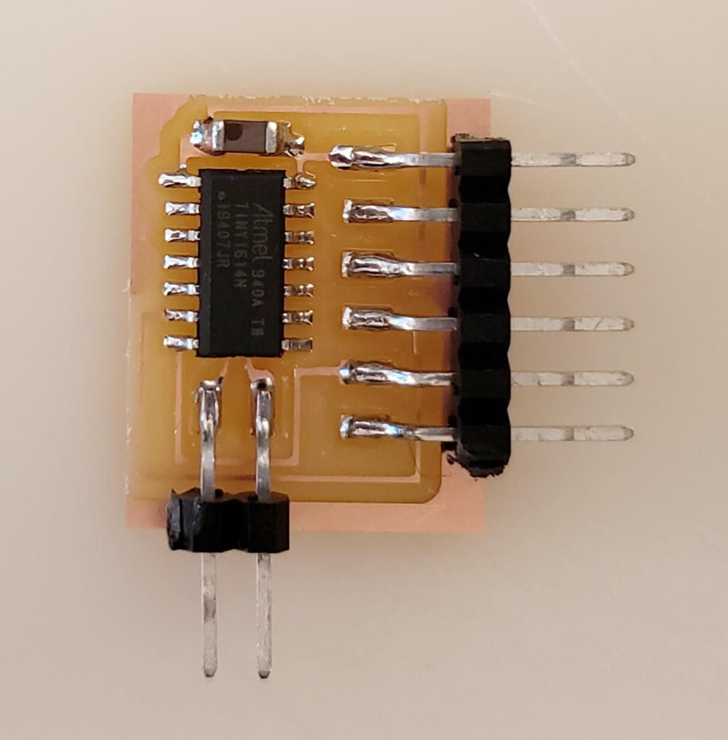
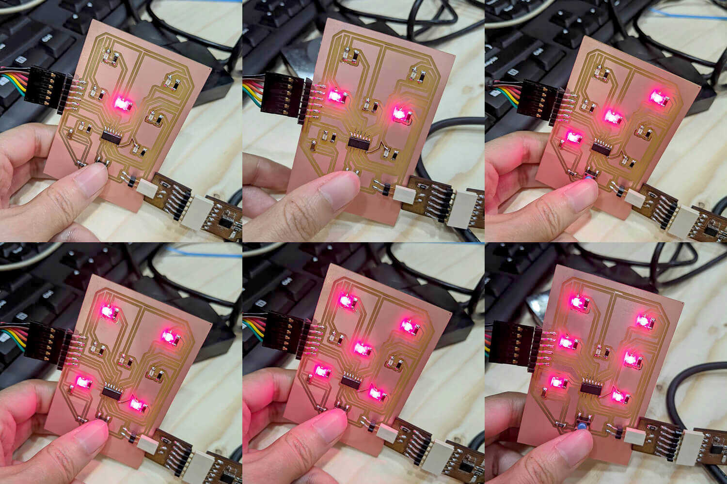
I intend to make an LED dice as a concrete project during this week and the Embedded Programming week in order to fully understand the electronics design, production, and embedded programming process. This week's goal will simply be turning on/off all the LEDs when pressing a button, and displaying random numbers will be the main task for the 8th week.
I chose to start with an ATtiny1614 hello-world board after being consulted by Santi and Josep. In summary, the ESP ones are unnecessary complex and the sample ATtiny1614 board has FTDI/UPDI headers which means I could use the outcomes of the 4th week to talk to it. ATtiny1614 means the chip has 16 KiB flash memory and 14 pins, which seemed to be suitable since I need 2 pins for VCC and GND, 1 pin for UPDI header, 2 pins for FTDI serial header, 7 pins for 7 LEDs and 1 pin for 1 button. The chip was also recommended by Neil as a good one to start with.
Managing libraries
As mentioned above, I used KiCad to design my PCB. The instructors also provided us with a useful Fab library adapted for SMD components and KiCad V5.0:
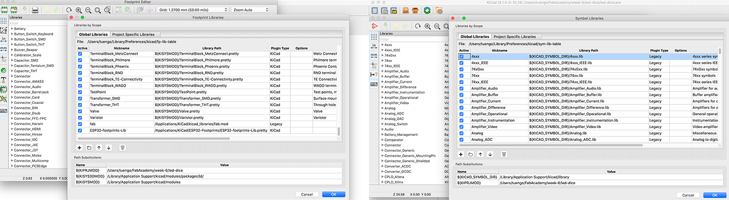
I simply followed Oscar's instructions to import all of the symbol and footprint libraries. However, in the Connectors library included in KiCad V5.0, there is an AVR-UPDI-6 symbol with 6 pins (instead of 2 pins as the sample hello-world board). This UPDI component is also not linked to any footprint. That's why I decided to create a custom UPDI-SMD-HEADER symbol and a custom fab-1X02SMD footprint.
To do that, the first step was to modify the fab-1X06SMD footprint (which links to the FTDI header) in Footprint Editor. I deleted the pad no.1, no.2, no.5, no.6, and renamed pad no.3 and no. 4 to "1" and "2". Then I exported it as a new footprint named fab-1X02SMD and imported the new footprint to Footprint Libraries.
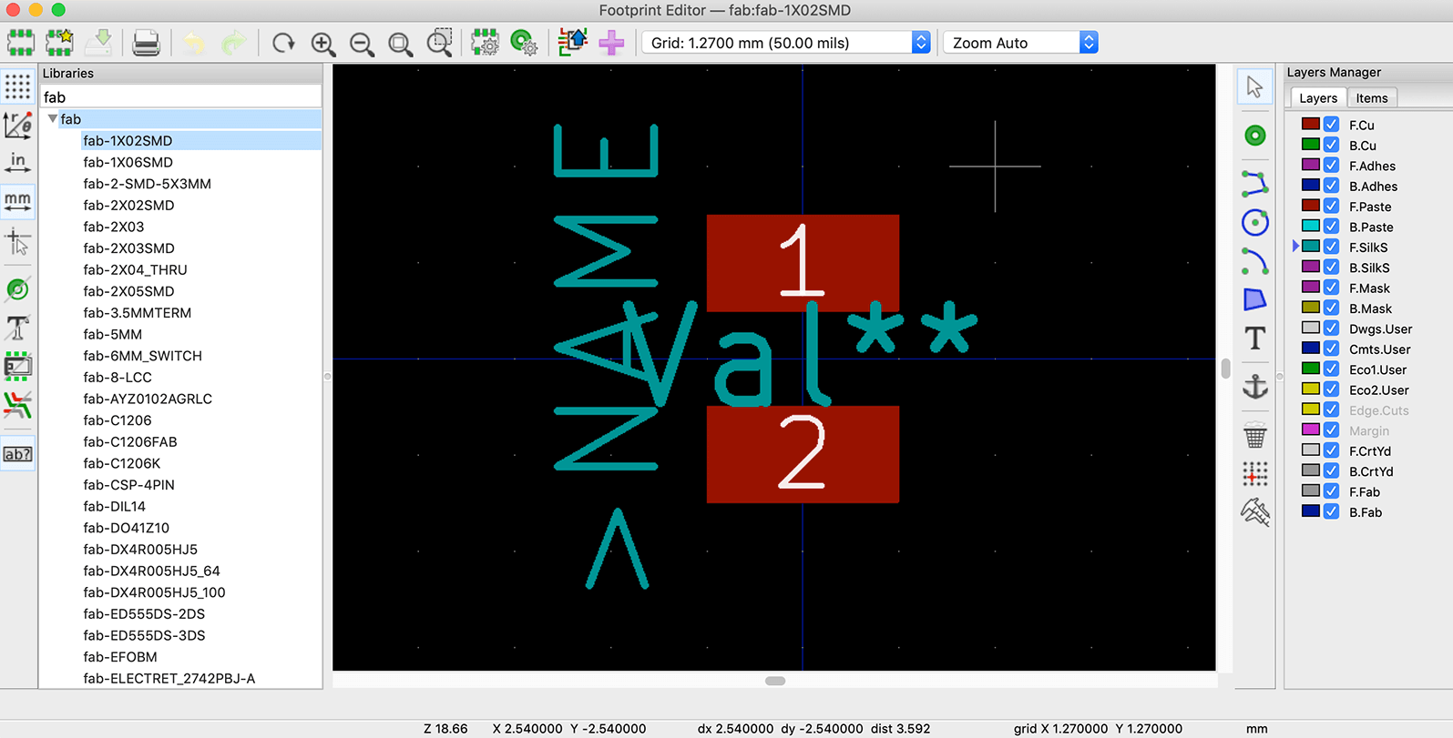
Next step was to input an $INDEX of fab-1X02SMD to the fab.mod file. In the same file, I added a new $MODULE:
    $INDEX
    fab-1X02SMD
    $MODULE fab-1X02SMD
    Po 0 0 0 15 00200000 00000000 ~~
    Li fab-1X06SMD
    Cd
    Kw
    Sc 00000000
    Op 0 0 0
    At SMD
    T0 -1000 0 500 500 900 40 N V 21 N ">NAME"
    $PAD
    Sh "1" R 1000 500 0 0 0
    Dr 0 0 0
    At SMD N 00888000
    Ne 0 ""
    Po 0 -500
    $EndPAD
    $PAD
    Sh "2" R 1000 500 0 0 0
    Dr 0 0 0
    At SMD N 00888000
    Ne 0 ""
    Po 0 500
    $EndPAD
    $EndMODULE 1X02SMD
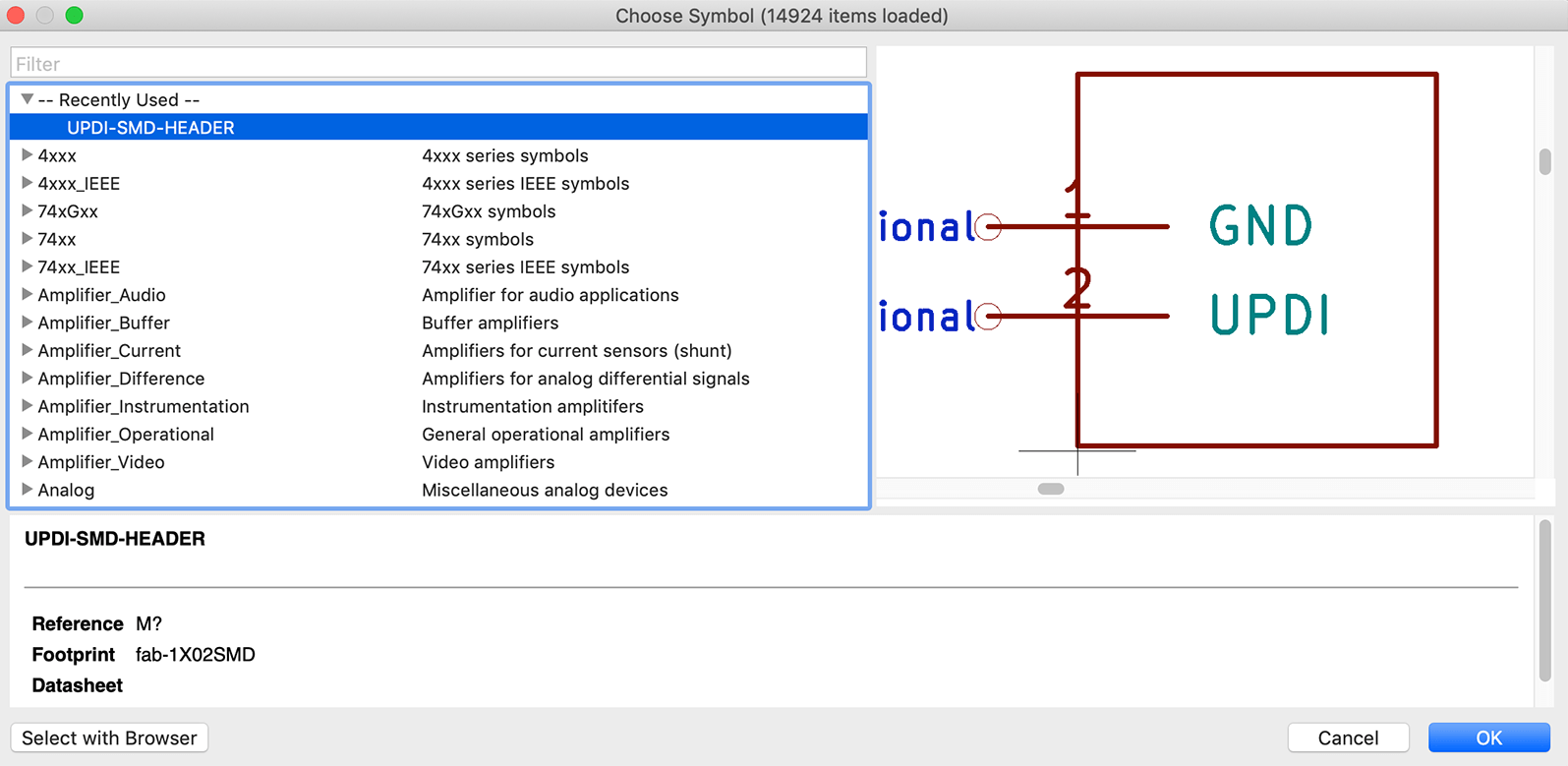
I also added a new $DEF to the fab.lib file in order to create a new custom UPDI-SMD-HEADER symbol linked to the custom footprint:
    DEF UPDI-SMD-HEADER M 0 40 Y Y 1 L N
    F0 "M" 0 0 45 H I C CNN
    F1 "UPDI-SMD-HEADER" 0 0 45 H I C CNN
    F2 "fab-1X02SMD" 30 150 20 H I C CNN
    $FPLIST
    *1X02SMD*
    $ENDFPLIST
    DRAW
    P 2 1 0 0 500 670 100 670 N
    P 2 1 0 0 100 670 100 255 N
    P 2 1 0 0 100 255 500 255 N
    P 2 1 0 0 500 255 500 670 N
    X UPDI 2 0 400 200 R 40 40 1 1 B
    X GND 1 0 500 200 R 40 40 1 1 B
    ENDDRAW
    ENDDEF
Finally I had the new self-made UPDI symbol and footprint!
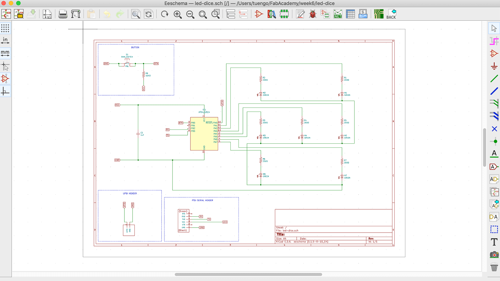
Designing schema with KiCad Eeschema
I started with sketching my board in the Eeschema schematic editor first. To understand the ATtiny1614 chip and its pins, I refer to the data sheet here. The workflow went like:
- Create new
.proKiCad project and open the.schfile in Eeschema - Choose the Place component tool and select the components needed from the libraries. The components I used: ATtiny1614-SS for the IC, FTDI-SMD-HEADER for the FTDI header, 6MM_SWITCH6mm_SWITCH for the button, CAP-UNPOLARIZEDFAB for the capacitor, RES-US1206FAB for the resistors, LEDFAB1206 for the LEDs, and my custom UPDI-SMD-HEADER for the UPDI header.
- Edit the properties of the components (annotations, values, and footprints) by hovering and press E. In order to calculate the resistance value of the resistors, I also took a look at this data sheet.
- Arrange related components to some basic building blocks: FTDI SERIAL HEADER, UPDI HEADER, and BUTTON.
- Choose the Place global label tool in order to assign some global "labels", such as GND or VCC, BTN or UPDI, etc. Separating blocks and wiring them (by pressing W to begin wire and K to end wire) with those global labels can make the schema more readable.
- As common practices, add a pull-up resitor to the BUTTON block (in order to stabilize measurements while reading inputs) and wire a capacitor parallelly with the power supply (in order to avoid voltage fluctuations).
- The final step was to Generate Netlist. Netlist serves as a link between the schema and the PCB layout.
Here you go all the components displayed and wired together!
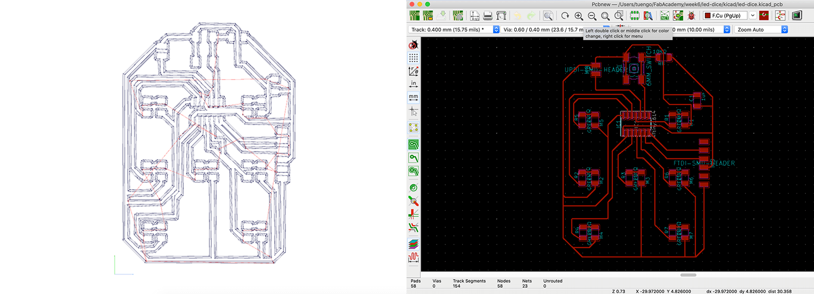
Designing PCB with KiCad PCBnew
When I Read Netlist in the PCB layout editor PCBnew of KiCAD, I immediately saw a horrible tangled mess. The workflow used to save myself from that basically included 2 steps of Placement and Routing:
- Re-arrange the components: select pads from the footprints and press M to move them or press R to rotate/flip them. By taking a look at the white lines, I could more or less imagine whether my components could be routed easily.
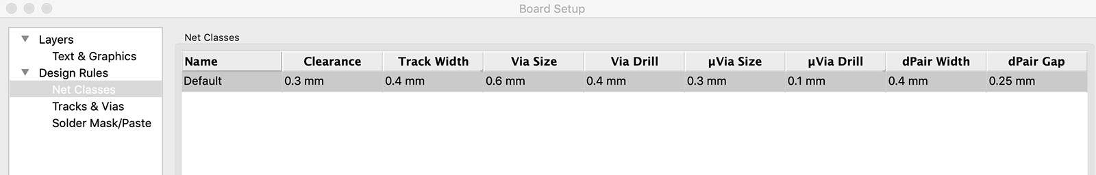
- Set the proper Design Rules complying with the 1/64 milling bit. The set of rules was provided by our instructors.
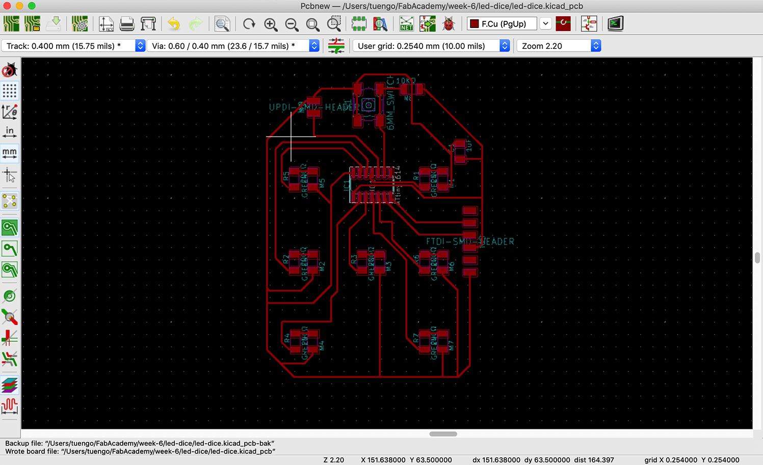
- Use the Route tracks tool to draw traces that connected the pins of the components. I started with the IC and the LEDs first. Sometimes I modified the schema, generate the Netlist and read it again in order to solve some crossed traces.
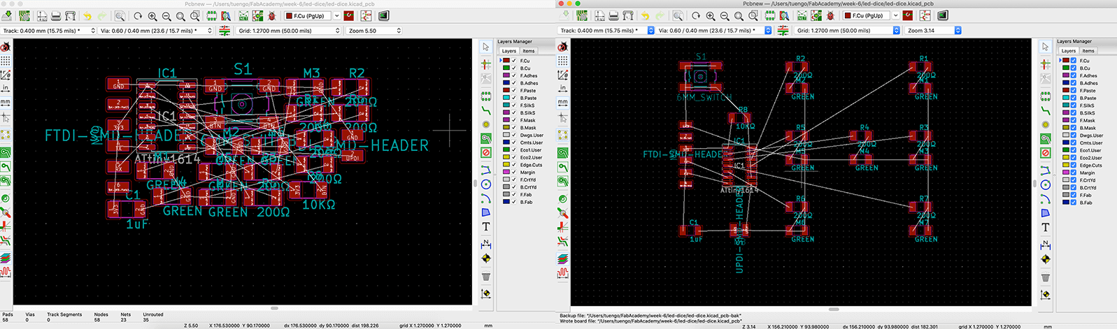
After struggling for a while, a good tip I learned was to connect all components with VCC pins first. The connections between GND pins should be done after the others, and they can be joined to form an overall shape of the layout.
Electrical and design rules check
KiCad includes an Electrical Rule Checker in Eeschema and a Design Rule Check Control in PCBnew that are dedicated for sign-off checks. The LVS verification is included in DRC Control.
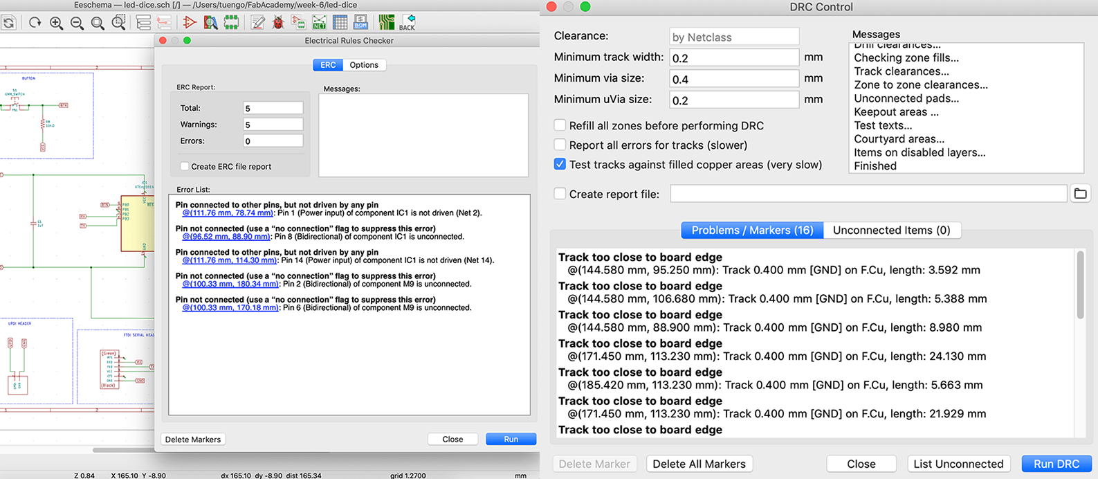
Basically, no news is good news. However, I still had some issues which were indeed OK. For example, the ERC complained that I had some unused pins in the schema, and since I didn't create an edge cut in PCBnew, the DRC mistook the outer traces as the edge of the design.
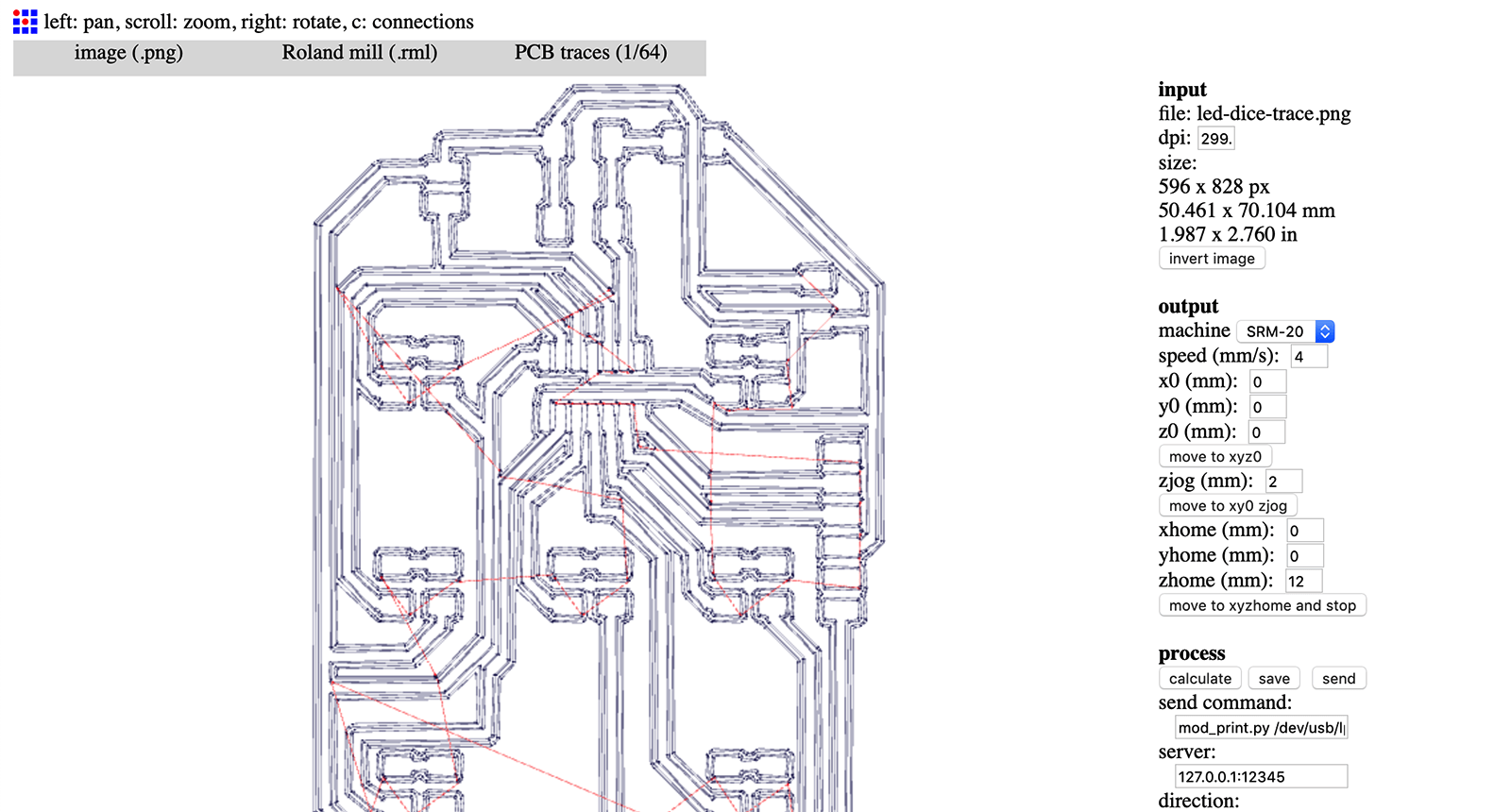
Generating toolpath with Fab Modules
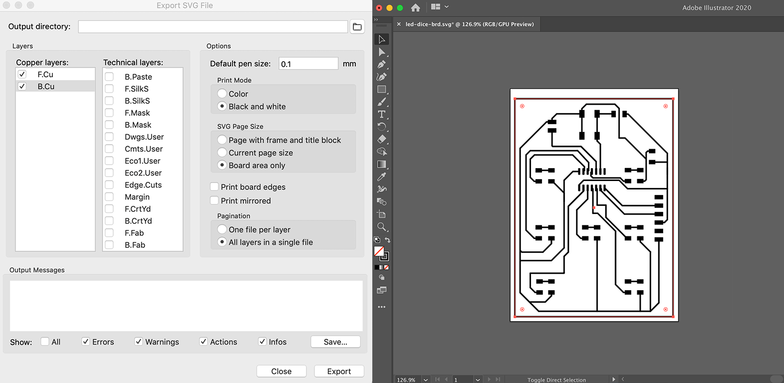
The common file format to be sent for manufacturing would be a .gbr file. However, since I've already been used to Fab Modules, I continued using it to generate the toolpath using exported .png files. Before doing that, I had to export an .svg file from PCBnew and modified it in Illustrator, then exported the .svg file to .png.
The next steps in Fab Modules were similar to what I did in the 4th week. However, after generating the toolpath in Fab Modules, I could spot some unwanted joined traces, and the reason was that they were too close together in the PCB layout. Hence, I had to go back to PCBnew to modify those naughty traces.
After checking again in Fab Modules, everything seemed to be alright:
Ready to fabricate!
Milling and soldering
And the nightmare came.
Although I passed the design rules check, the .rml file seemed to be good in Fab Modules, and the workflow was similar to what I did in the 4th week, there were still MANY troubles when it comes to production. I tried 5 times with different SRM-20 machines available at the Fab Lab, and basically faced all these below issues:
- The trace width was obviously thinner than 0.4mm, which could lead to issues if they will have to carry a high current later.
- Both the widths of the traces and the gaps between them were inconsistent. From what I see, the inner traces where there was high density were thinner and more unstable. This was the weirdest thing that I didn't understand because I assumed that even if I did something wrong with the settings, it supposed to maintain the same width of all traces(?)
- The cutting depth is not consistent: some parts were milled through completely, some were not. This could be a problem with the milling bed.
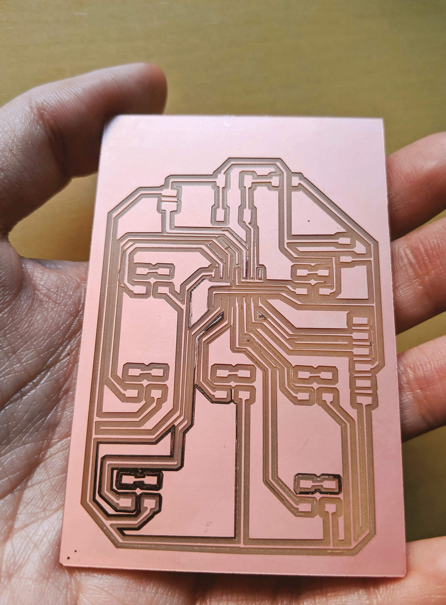
In order to "debug" this, I tried to go back and check every single step I did. All the trace widths in PCBnew were exactly 0.4mm, and our instructors recommended to keep it like that. All exported .svg lines had the same 0.4mm width. The settings of Fab Modules were exactly the same as my classmates' designs. Then I figured out that I didn't export my .png with + 500dpi resolution. I was not so certain whether this was the main reason since resolution seems to affect not the width of the horizontal and vertical traces but the 45° ones or the shapes of the pads. However, I still continued to mill another one with 1000dpi resolution, because it could be something I didn't understand about the way Fab Modules calculates the toolpath.
The above-mentioned issues still happened. However, the result came out much cleaner than before and after testing with the multimeter, everything was OK. Hence, I went ahead with soldering it!
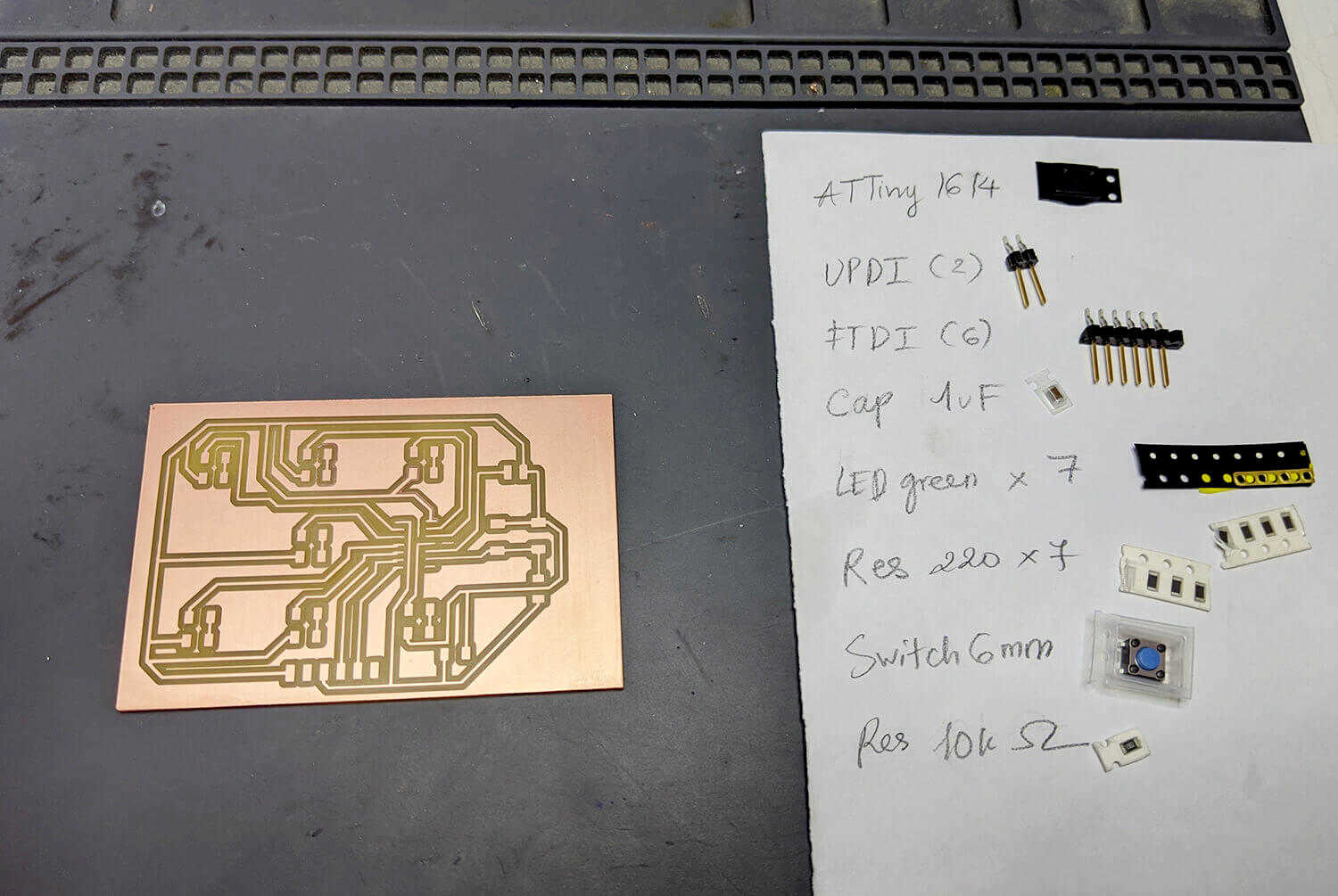
Not much to say about soldering. I only have some highlights regarding the soldering direction of the components: the cathode side of an LED is marked with a tiny green line, the dot in the IC indicates VCC pin, and we should pay attention to the connected legs of the button. Besides, I used the 220Ω resistors (instead of 200Ω ones as in the design) and red LEDs (instead of green ones) due to stockout issues.
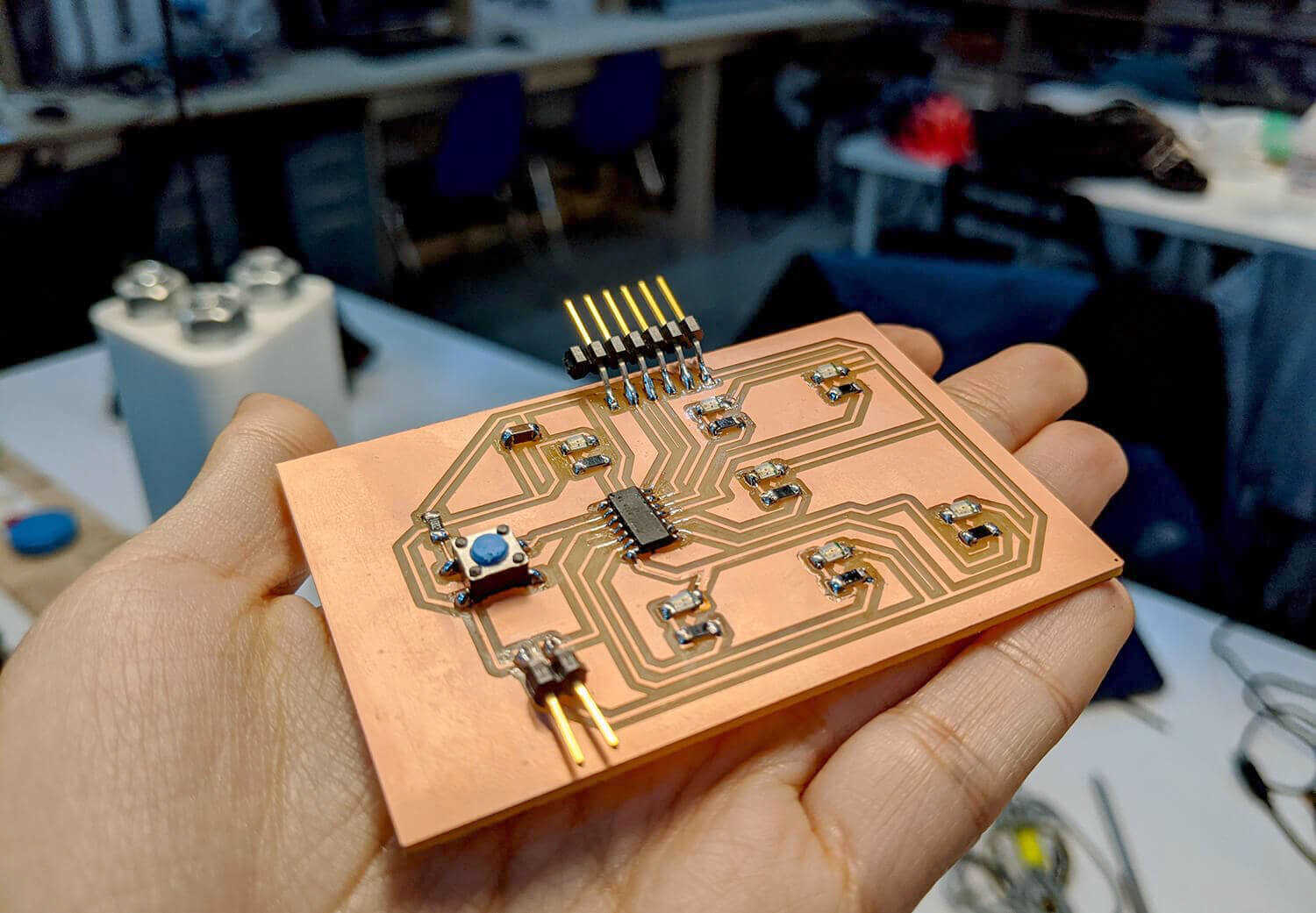
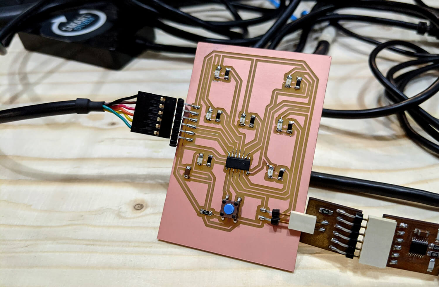
Then I can used the FTDI and UPDI made in the 4th week to program the board!
Programming with Arduino IDE
I chose Arduino IDE to program my board since it was easy to use for a newbie like me. I simply followed this tutorial to install megaTinyCore to my Arduino IDE, and I used pyupdi driver to program my LED dice with UPDI interface.
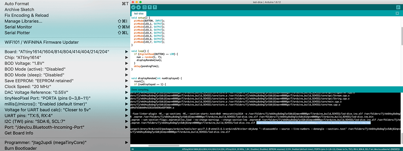
As mentioned at the beginning of the assignment, I only intended to turn all the LEDs on this week. However, writing the code for a working LED dice is quite easy, therefore I went ahead with finishing it. I would like to document this part better in the 8th week. The first reason was that I want to focus this week on EDA design flows only. Besides, in the 8th week, I will try to get an overview of programming my LED dice in different languages and environments, or I will think of other games that could use a button and 7 LEDs. The only limit is the imagination, rite?
Group assignment - Test a board with the multimeter
Since our class couldn't do the group test together, I tried to fulfill this assignment by testing my fabricated board with the multimeter. Before doing that, I took a look at this useful tutorial in order to understand what I was going to test.
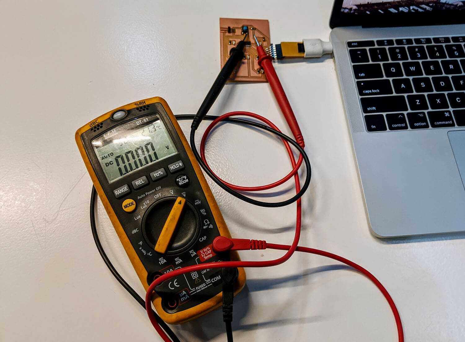
In summary, before plugging the board to the computer, using a multimeter we can measure:
- Voltage, resistance, current: rotate the knob to select what to measure, connect each probe on each side of the target component to be measured, and the multimeter should display the related value. Voltage and resistance can be measured by "wiring" the multimeter in parallel, while current must be measured by "wiring" the multimeter in series.
- Electronic continuity: check whether two lines are connected and the multimeter is supposed to be in beep-beep mode.
Conclusion
In general, it was an exciting week and I was so happy to have my first electronic something. There are only a few things I don't like about KiCad:
- Confusing library management and third-party library support
- Lack of an easy way to automatically update between the schematic and PCB layout
- Lack of an efficient interactive drag to move components without losing the routed tracks
I know that it might take me more time to feel comfortable with electronics in general, but this could be an incredible start for my future projects. Stay tuned!