6. Electronics Design
This week, I tried designing the echo hello-world board using EAGLE and then milling and soldering the board, and lastly, programming to function my board.
Assignments
group assignment:
- Use the test equipment in your lab to observe the operation of a micro-controller circuit board
individual assignment:
- Redraw an echo hello-world board, add (at least) a button and LED (with current-limiting resistor)
- Check the design rules, make it, and test it
- extra credit: simulate its operation
X. Group Assignment
Link to group session page.
X. Individual Assignment
1. Design a circuit 
Materials
None
Tools
- PCB Design Software: EAGLE
Workflow
Download and activate a library
I used EAGLE Free ver. for designing a circuit.
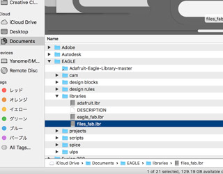
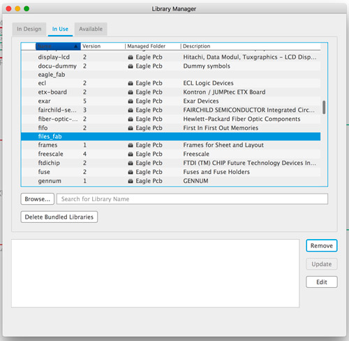
To show the icon of electronic pats, I downloaded the library from here and put them to the directory EAGLE -> libraries.
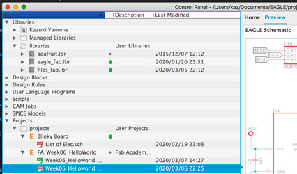
It needs to activate the library to use by clicking lump button at control panel. Control panel is automatically opened as opening EAGLE. Green lump shows activate and grey shows non-active.
Design a circuit diagram
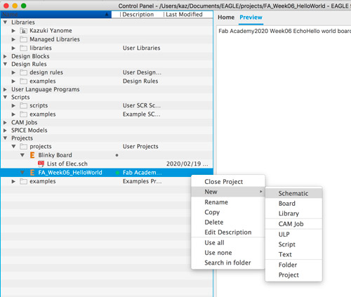
Created a new project in Projects -> projects directory.
Project consists of Schematic panel and Board panel. Schematic panel is the panel to design and assign a circuit diagram of PCB and Board panel is the panel to decide the connection and position of electric components.
So, first, created Schematic in my project by right-clicking the project I made, and opened Schematic panel.
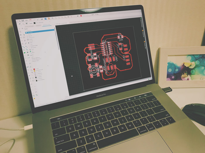
Here is Schematic panel.
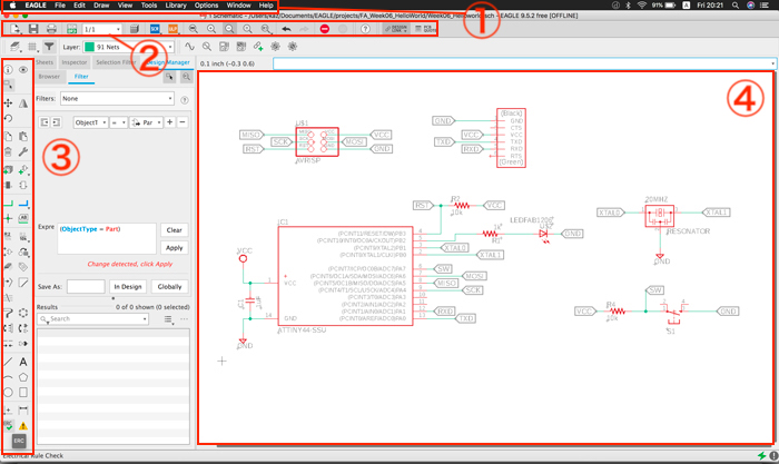
① Tool bar: All operations and commands can be performed from tool bar.
② New File, Save, Print, Switch screen etc.
③ Editor commands: Drawing tools
④ Work space
Please check if the library you downloaded is used properly.
Tool bar: Library -> Open library manager
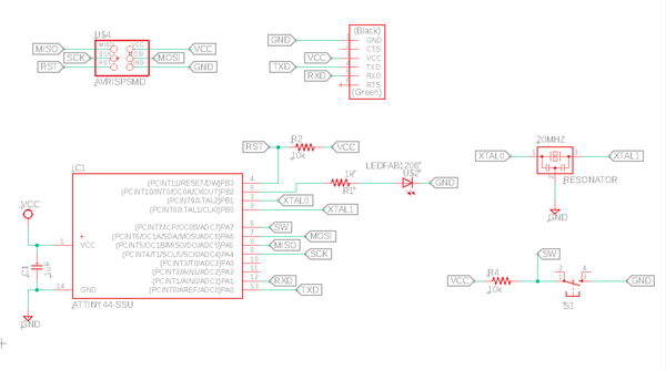
Referring the circuit sample, I re-designed the circuit diagram for the echo hello-world board.
Reference board is below;
Introduced the main commands that I often use at the circuit drawing.
Main Commands;
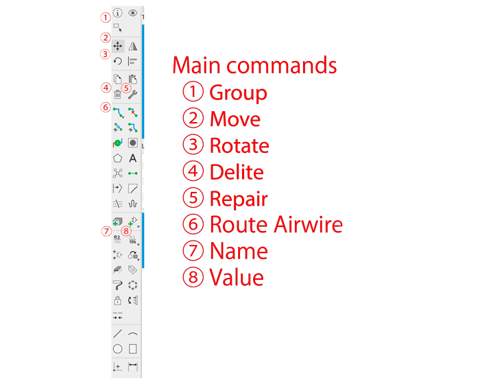
-
Group
To select some electronic parts at once. -
Move
To move a electronic part or an air wire. -
Rotate
To rotate a electronic part. -
Delete
To delete a electronic part or an air wire -
Repair
To change the width of air wires.
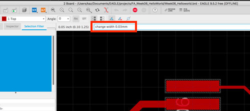
Tip
Command line
To change the width of air wires, I use the command line. To input change width OO mm and click the place you’d like to change the width, you can change it. The point is that you can change the plural air wires by just clicking them.
-
Route Air wire
To route air wires. Connect the electronic parts using the air wires.
The milling machine mills along with the air wires. -
Name
To name the electronic parts to be easy to distinguish each electronic part. -
Value
To assign a value optionally to be easy to distinguish the constant of each electronic part like the value of a resistance or capacitance.
Components:
| Components | PCS | NOTES |
|---|---|---|
| ATtiny44 | 1 | — |
| Resonator 20 MHz | 1 | For giving the timing clock frequency to IC |
| Capacitor 1 μF | 1 | For removing noise |
| Resistor 1 kΩ | 1 | For adjusting the current flowing to LED |
| Resistor 10 kΩ | 2 | ① For pulling up ② For pulling up |
| LED | 1 | — |
| Switch | 1 | — |
| Pin for FTDI | 1 | 6 pins / 1 pcs |
| Pin for AVR ISP | 1 | 6 pins / 1 pcs |
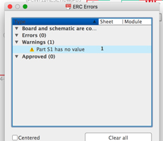
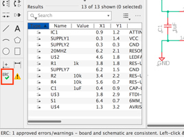
After finished the design, I checked if all the electronic components are connected properly by myself. And then I did ERC (Electrical Rule Check) to check if there are any problems or errors in the designed circuit.
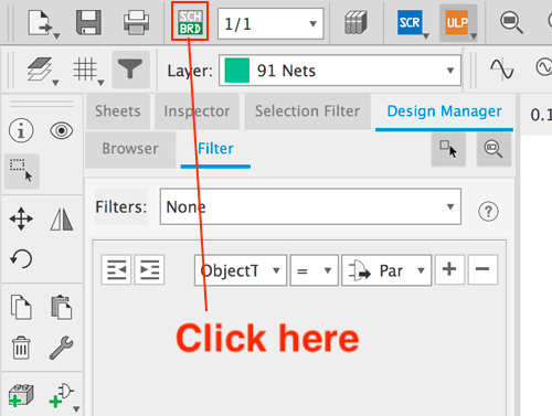
If all the check has done, go to Board panel!
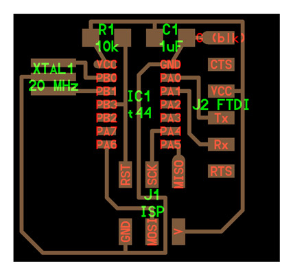
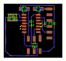
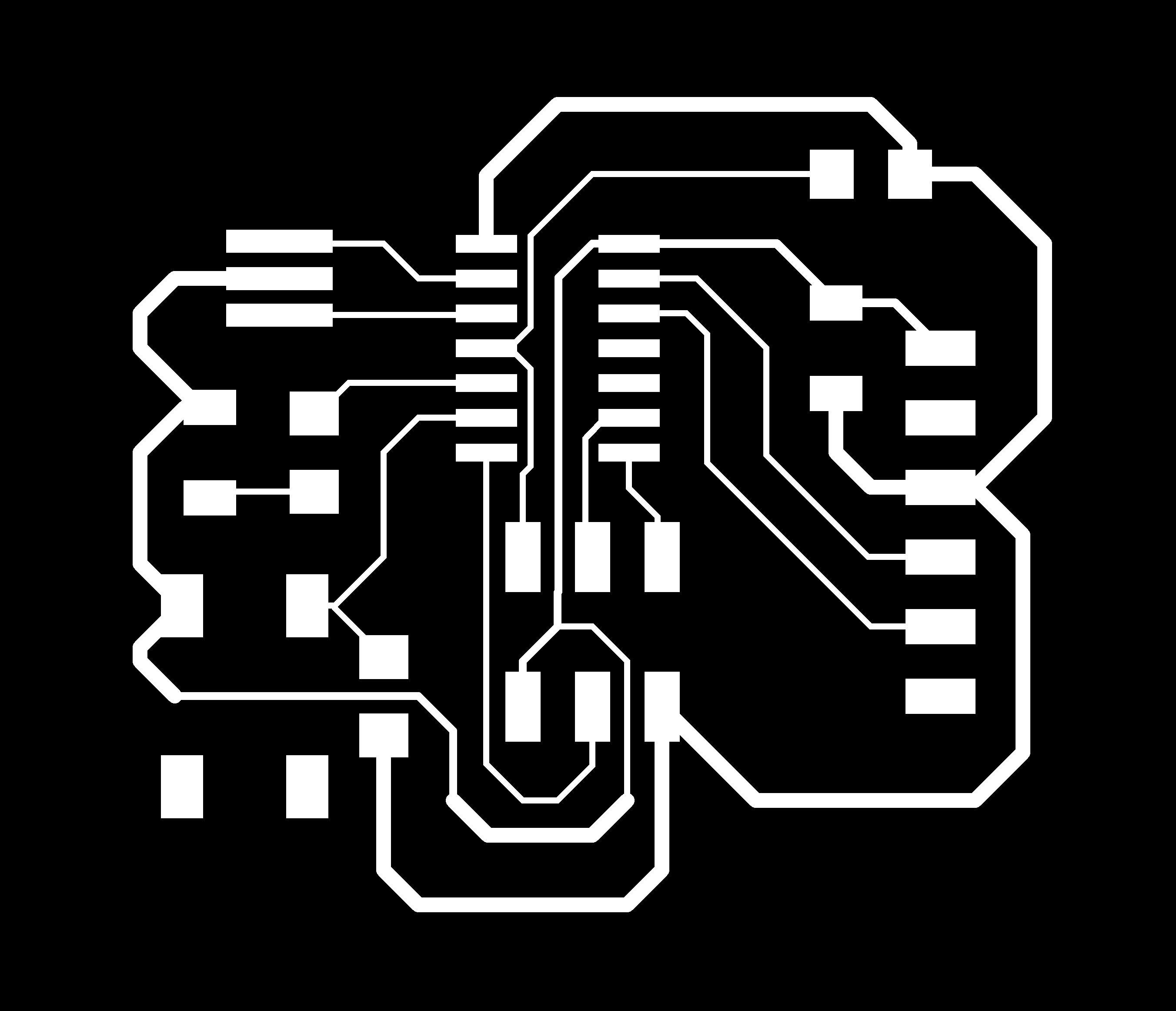
Adjust the position and wiring of electronic components
Go to board panel by clicking Generate/switch icon.
You can also move between schematic and board panels from this icon.
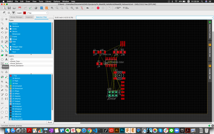
Here is Board panel.
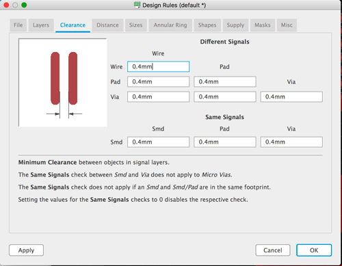
Set the design rules before wiring.
I adjusted clearance between components. Go to Tool bar: Edit -> Design Rules -> Clearance and input 0.4 mm to all the parameters. This means you can’t put the electronic components for the region of 0.4 mm from other electronic components or wires.
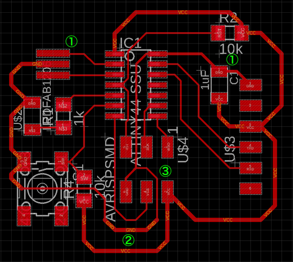
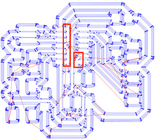
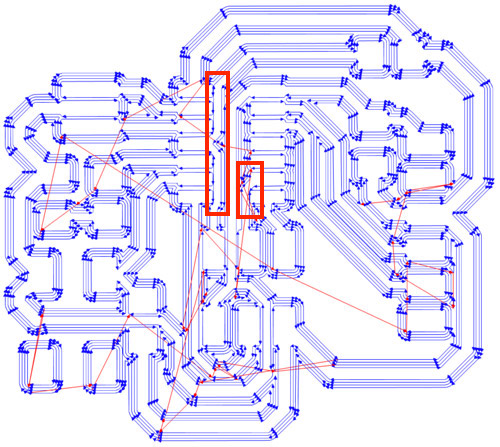
My wiring result is below.
There are so many tips with wiring.
Tip
① Position of Capacitor and Resonator (Impedance of copper pattern)
Make sure that the capacitor is placed near the component you’d like to remove the noise in order to decrease the Impedance of a copper pattern as possible. It means the longer wiring pattern generates so much noise. So, in my case, I put a capacitor and a resonator near the ATtiny 44 micro-controller.
Tip
② Thicken Vcc and GND line two times than the other signal line
Due to decreasing the Impedance of a copper noise.
Note
③ Don’t pass the wire between the connection pins
As the wire are passed between the connection pins and the board are communicating with other board using those pins, the communication signals affects the wire passed between pins as the noise.
Note
Design the corner of every pattern bigger than 90° for milling
If there are the corners smaller than 90° in your pattern, at the milling process the line becomes thin than you expected.
Note
Don’t put the noise-sensitive components near the noise-source
IC or Motor generate the noises during their operation. So as you put the noise-sensitive components like analog sensors near those noise-source, they are affected from the noise and doesn’t work properly.
Don’t forget to perform ERC and DRC (Design Rule Check).
If No error was shown, go next!!
Export a pattern diagram as .png files
To read .png file to Mods and mill it, I wanted to export the pattern diagram as .png file. But before that, some procedure are needed. I made two .png files to mill. One is the pattern. Another is the frame to cutout.
For the frame, I adjusted the frame for cutout first and showed only dimension layer which draw the cutout frame, and then export it by going to tool bar: File -> Export -> Image.


2. Milling & Soldering
Materials
- Copper Board
- Electronic Components
- Solder
Tools
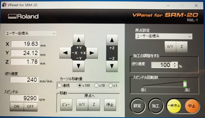
- Milling Machine: SRM-20 (ROLAND)
- Endmill (Size -> Pattern: 1/64 Frame: 1/32)
- electronic components
For milling, all I did were the same as week4 page. So please check it.
Failure
The pass cannot be through the smaller space than the endmill’s size
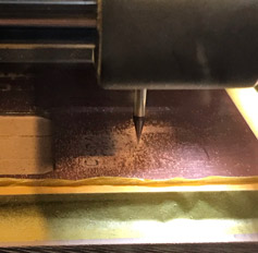
Note to check if all the passes are through before milling your board. I didn’t check them so the mill cannot be through between the IC pad and the line under the IC.
So I had to cut those parts using a super sonic cutter.
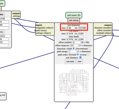
2020/7/28 Additional
Revised the tool diameter value on MODS
I checked that the tool path cannot be passed. To pass the tool path, I tried revising the tool diameter value from 0.39624 mm as default with 1/64 mill to 0.38 mm.
It resulted in that the tool path can be passed because MODS recognized that the diameter of mill is smaller than default and can pass the tool path between the narrow space.
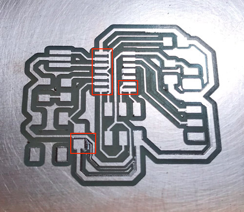
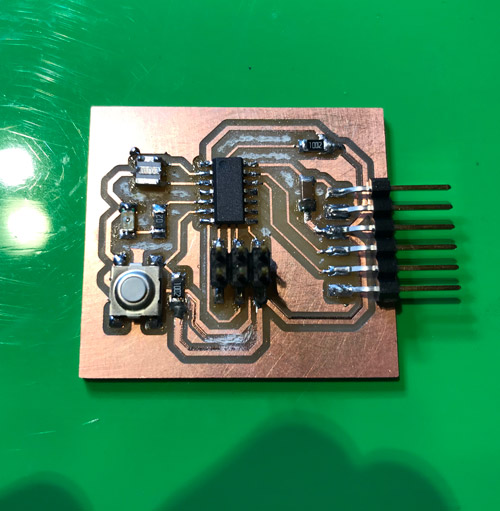
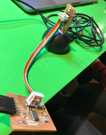
Here is the result of my soldering.
I soldered a little too much… But I checked that all the components are conducted with copper pattern using a multimeter.
Okay, move to programming chapter!
3. Programming
Materials
- Connector and Lead Wire
- Program
Tools
- Hello-world board: Micro-controller -> ATtiny44
- Writer (used made at week4)
- Arduino (downloaded)
In this chapter, I’ll explain how my board can return the characters inputted from my PC using Arduino.
First, I have to write the program to return the characters to my hello-world board using the writer which I made at week4.
Downloaded the hello.ftdi.44.echo.c and hello.ftdi.44.echo.c.make programs from link and put them into the same folder.
You can downloaded the programs that I used from the below links.
Files - hello.ftdi.44.echo: .c and .make
Make sure to connect the connector with the correct direction.
After I connected my board, writer, and my PC, I opened terminal and ran three commands in order.
make -f hello.ftdi.44.echo.c.make
make -f hello.ftdi.44.echo.c.make program-usbtiny-fuses
make -f hello.ftdi.44.echo.c.make program-usbtiny
I succeeded to write the program to my board without bugs.
(Actually, I’d like to debug for learnning…)
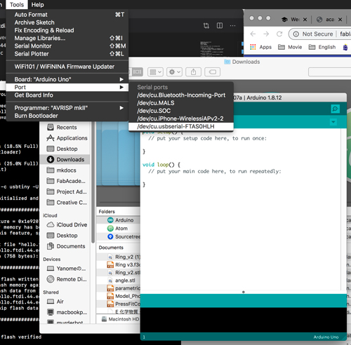
So next, I downloaded Arduino and opened it.
Then selected the port: /dev/cu.usbserial-FTAS0HLH from toolbar: tools -> Port.
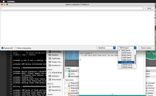
Clicked Serial Monitor and then selected 115200 baud.
Finally, I inputted Hello by each character and confirmed that my board returned their characters on the screen.
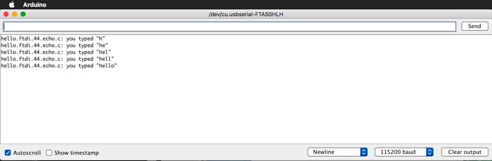
So…Finish!!
3. Conclusions
Submission
Self-reviews
1. This week’s work
This week, I had no bugs and succeeded all the process smoothly. But most difficult thing for me was wiring a circuit diagram. It was like a puzzle. It took about 3 hours for me to finish wiring. Very complex and difficult… I thought that I’d like them to tell me if someone knows the tips about how to do those.
2. Project Management
Score (Max: 100)
-
Hierarchy: ?
This week, I proceeded almost processes manually watching tutorial. -
Triage: ?
-
Spiral Development: ?
-
Supply-side Time Management: 30
It took about 3 hours only to draw my circuit diagram and I didn’t start other things until I finished drawing. I should’ve take care of my whole time to work. -
Parallel Development: 80
I prepared for the next week’s local session while doing this week’s local session. I ask Hiroaki Kimura who is the student and familiar with wood materials and process which wood materials I should select for the next CCM week. And discussed my final project with other people.(Thank you!) -
Document as you work: 50
I sometimes forget to document when I was using the app.(EAGLE this week)
X. MEMO
What I wanted to learn more
-
What does those means:
FDTI(TXD, RXD), RST -
Programming
I followed only the process but I couldn’t understand it deeply. -
Computer Architectures
-
History of Computer science
-
in-system development
I don’t know the differences of ISP, UPDI, JTAG. -
What do ‘cores’ mean?
-
Micro controller
-
Python