5. ELECTRONICS PRODUCTION
This week I made the group assignment with my co-worker Álvaro Macián, we are both from Sedicupct-Fablab and our local Fabacademy node is FabLab León.
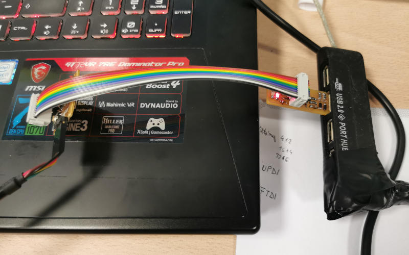
In my individual assignment, I have managed to make an in-circuit programmer by milling and stuffing PCB
I have continued using my weekly planning in which I have updated my activity in FabAcademy
This has been my work sequence during this week:
5.A. GROUP ASSIGNMENT
In my repository in each week in which a group assingment must be carried out, I include the documentation of the work done, but also the group work can be accessed on the Fablab website of which I am a remote student.
This is the link to access the space of group assignment from FABLAB León.
This is the work done in group
Characterize the design rules for our PCB production process
This group assignment was done by my partner Álvaro Macián and I together from our local node in Sedicupct-Fablab, we are remote students of the Fablab León node.
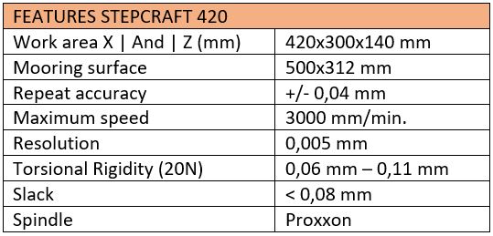
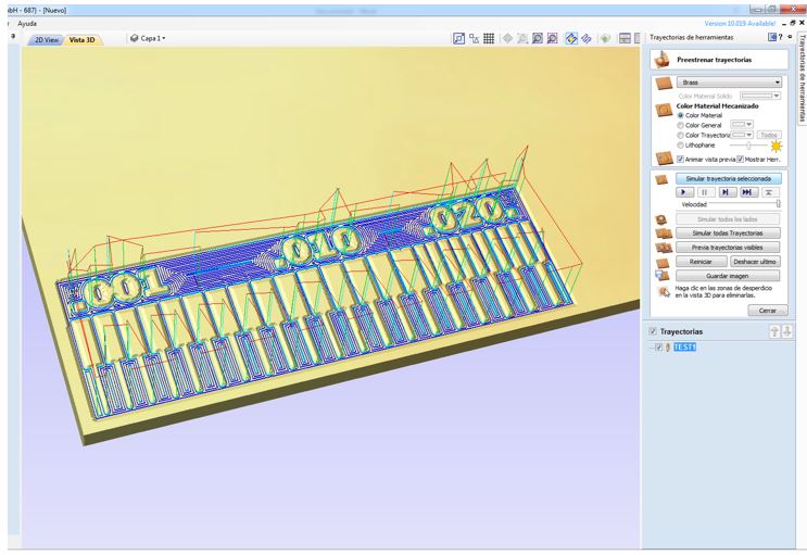
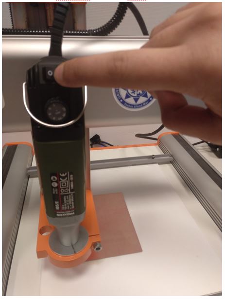
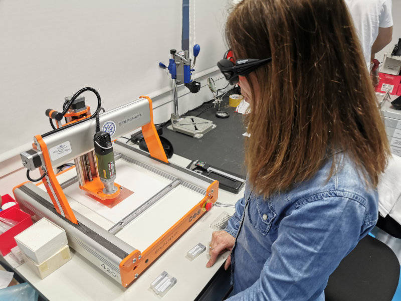
The PCB milling machine we have in the Sedicupct-Fablab is STEPCRAFT 420 .
It has interchangeable modules (laser engraving, 3d printing, milling machine, …) so it is very versatile. We had never used it to mill PCB so the assignment has been laborious.
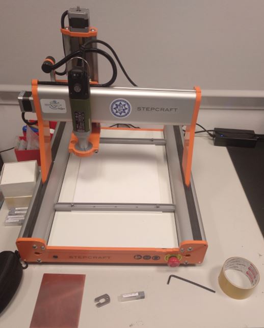
Important!!! In the initial tests the mills were always broken shortly after starting to mill. This was desperate. Mills broke because they were so long. When we bought the good ones, 2mm long, we were happy.
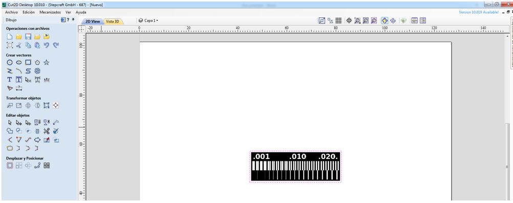
5.A.1. Resolution test
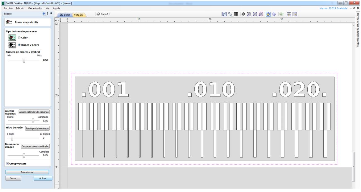
This is the image to test the resolution of the machine.

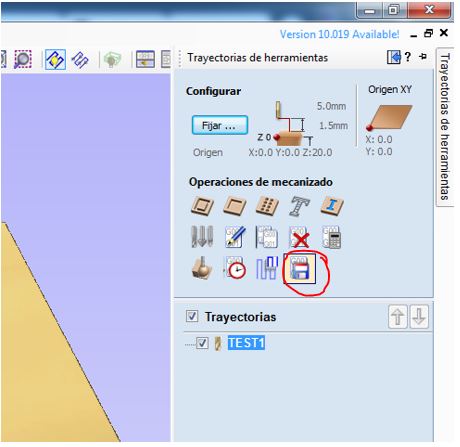
With the purchase of the milling machine we obtained the Vectric Cut2D software to generate the gcode and the UCCNC software for Stepcraft to control the milling machine.
Below are the steps to mill PCB with our software.
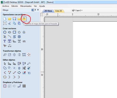
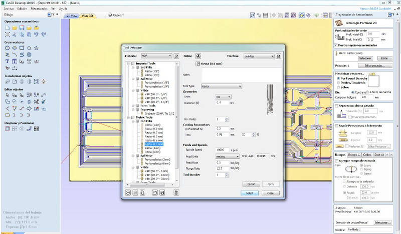
5.A.2. GCODE generation with Cut2D
-
Open Cut2D.
-
Configure the material.
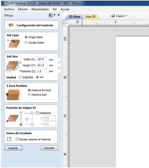
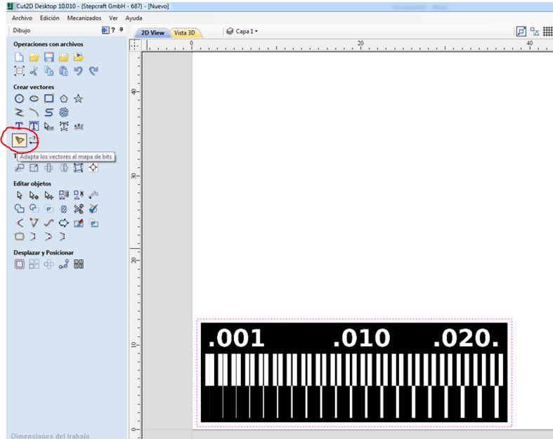
- Import the bitmap for plotting.
- Adapt vectors to the bitmap.
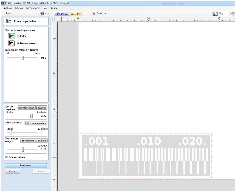
- Configure the machining operation. Select “Recessed Strategy”.
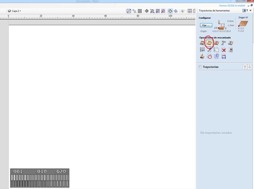
-
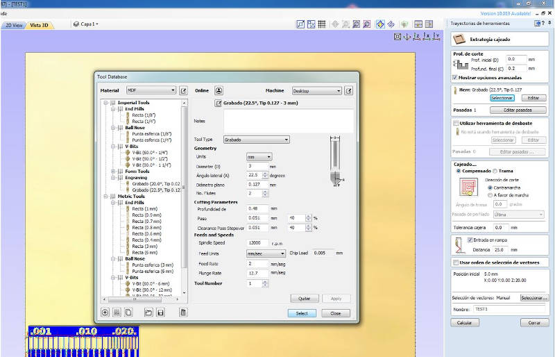
Select the tool and its parameters. Since we had never used the milling machine to make circuits we have looked for values to take as a reference for the parameters. In mods we saw that they use a feed rate of 4 mm/s for the Roland. We found another fablab with our same machine, Lakaz Lab, which used 0.5 mm / s. So we have tested different speeds (4, 3, 2, 0.5 mm/s) and the best result at the highest speed has been obtained with 2 mm/s.
- Feed rate = 2mm/s
- Cut depth = 0,2mm
- Speed spindle = 12000rpm
-
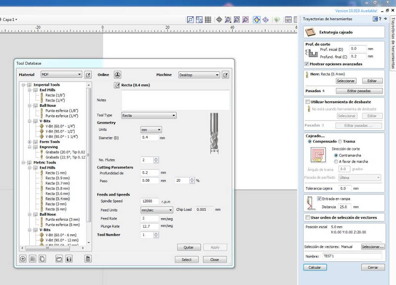
I have also tried with this other type of mill with the same parameters.
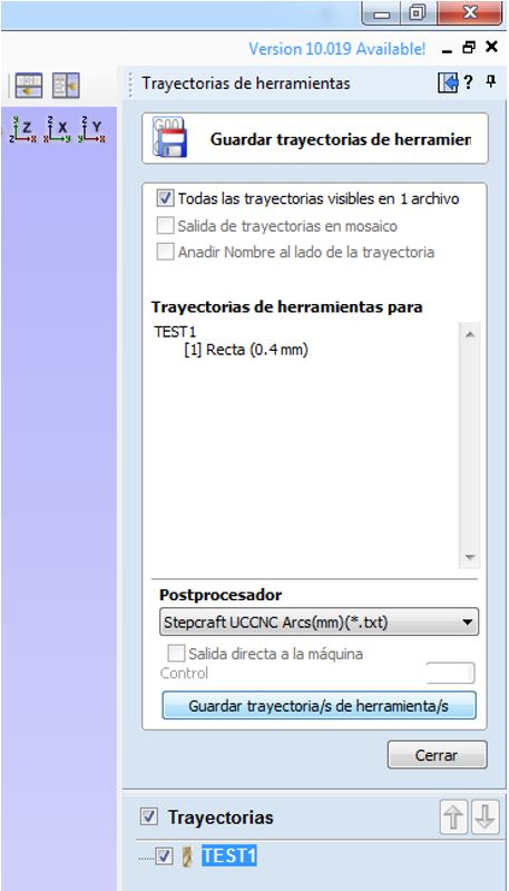
- And click on “calculate”. The GCODE is generated and we can visualize the operation.
- Save the GCODE in a text file.
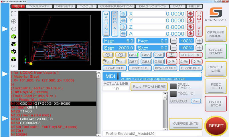
5.A.3. Machine preparation and control with UCCNC
-
Open UCCNC.
-
Click on “LOAD FILE” to open the gcode.
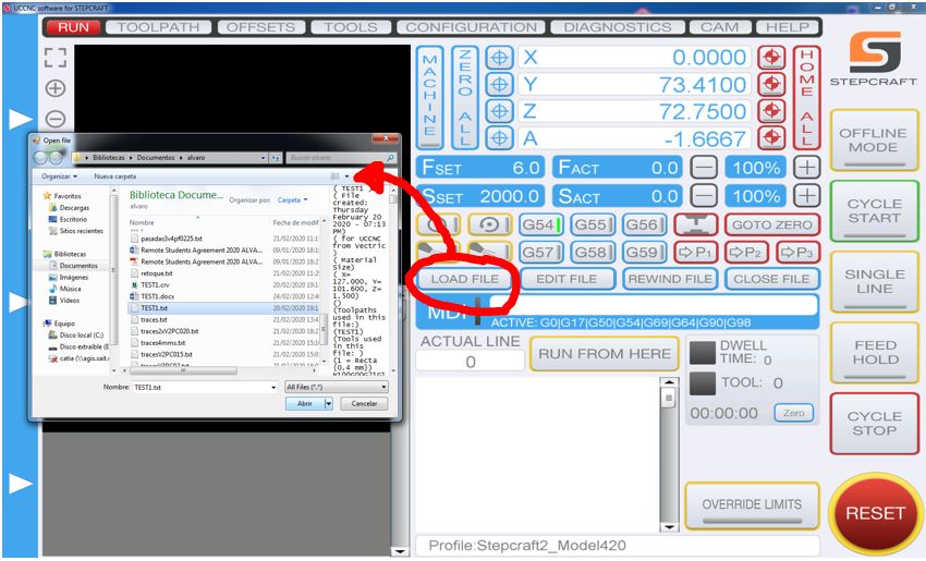
- Prepare the material and the mill. Use double-sided tape to fix the PCB to the milling table.
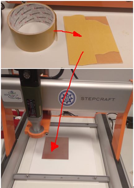
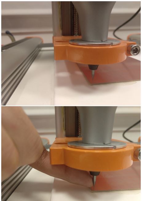
- Move the milling head manually with the left panel in UCCNC. Place the mill without tightening. Move the head closer to the top surface of the PCB. Loosen the mill and drop the mill until it touches the PCB. Use your finger so that the mill does not fall suddenly or it will break. Squeeze the mill. And mark the zero machine of the z axis. Raise the head a little and move in x and y as far as we want to place the zero machine.
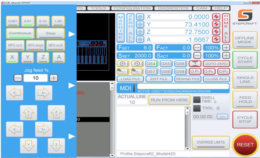
- Turn on the spindle and click on “CYCLE START”
5.A.4. Results
The following parameters have been used: - Feed rate = 2mm/s - Cut depth = 0,2mm - Speed spindle = 12000rpm
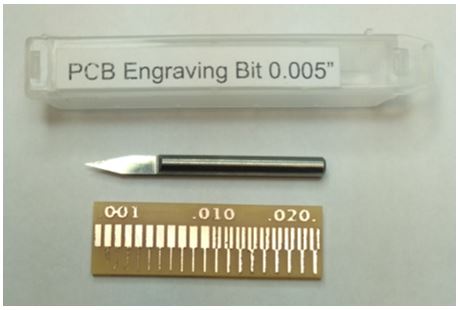
- Using the engraving Bit 0.005 ”resolution 0.004” on the outside line and 0.011 ”for the inside line.
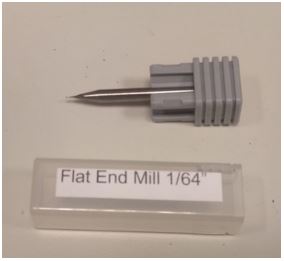
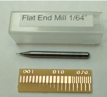
• Using the Flat End Mill 1/64 ”, the resolution 0.011” on the outside line and 0.016 ”for the inside line.
5.B. INDIVIDUAL ASSIGNMENT
Make an in-circuit programmer by milling and stuffing the PCB, test it, then optionally try other PCB processes
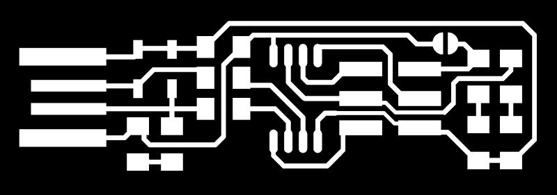
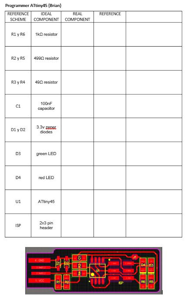
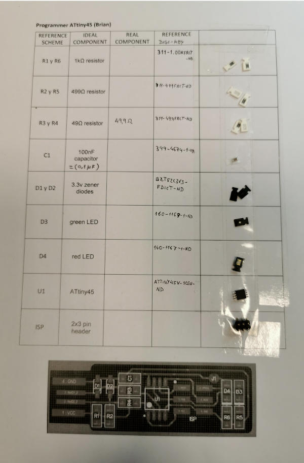
Our instructor, Nuria Robles, from Fablab León, has recommended us to make the programmer type ISP (AVR) Attiny45 version made by Brian, To start, because it is very well guided in your document and may be easier for us.
This is the image of the PCB to build.
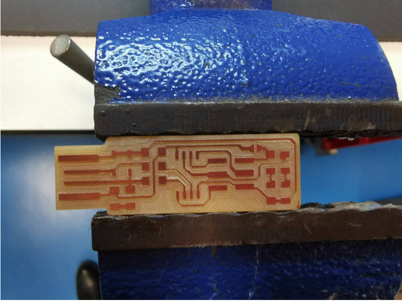
5.B.1. Milling process
I have prepared the STEPCRAFT 420 milling machine with the parameters characterized in the group assignment, which are the following:
- Feed rate = 2mm/s
- Cut depth = 0,2mm
- Speed spindle = 12000rpm
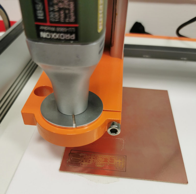
I have used Printed Circuit Board (PCB) Blanks, type FR-1.
From the Cut2D software I have configured the milling work of the board. Generating the GCODE of work.
With the UCCNC software, the generated GCODE is imported and the job is sent to the milling machine.
Now the machine works for me.
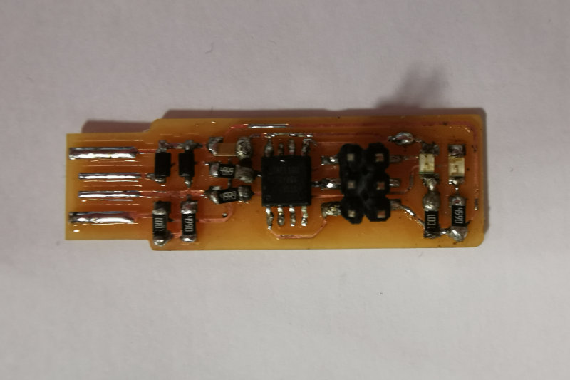
The result is this:
5.B.2. Welding process
I prepare all the components that I want to incorporate into my board to be able to turn it into a programmer. I order them and put them in a document that helps me organize these components (this is good advice from my instructor Nuria).
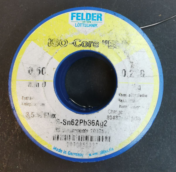
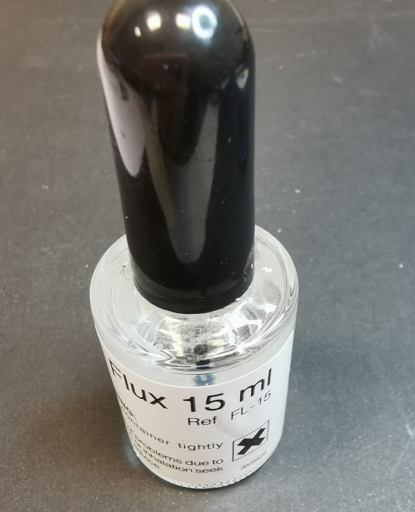
I use tin, a soldering iron (that I liked to have a finer tip), and a liquid called “Flux”, also known as a flux for welding is a chemical, usually in the form of fluid paste, which when applied on components that we are going to weld eliminates the rust between them substantially increasing the quality of welding. It also makes welding work much easier since it concentrates the heat and distributes it evenly in the work area.
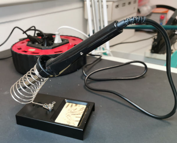
I place my board motionlessly and start the welding process, which I must say has been quite hard for me. It’s all very small and I don’t have what is said “a good vision.” I have used magnifying glass and light and everything in my power to optimize my work and be as careful as this work requires.
In fact I smashed a board and I had to start over because when welding the microcontroller I put together several pins with tin that I tried to remove when I tried to remove it.
I felt really awkward.
These are: “my first attempt” and “my board”.
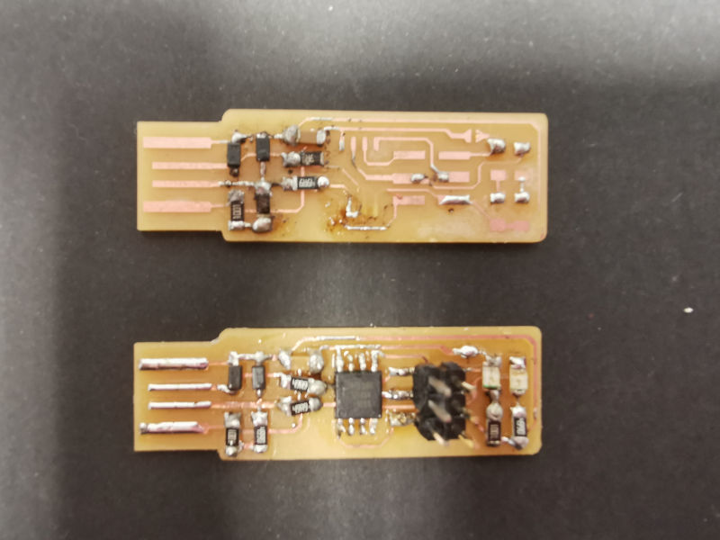
Even on the plate that was finally correct, my partner Álvaro had to help me solve a problem. He lost a piece of track (I don’t know how), and he with a piece of copper conductor of a wire, wrapped it in a stalk and sealed it replacing the track.
My torture ended like this:
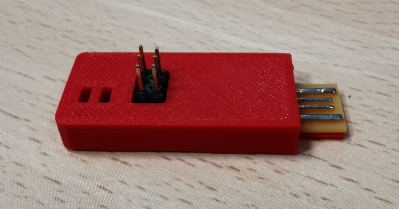
As I am so proud of my first PCB, I have manufactured a 3D print case to protect the circuit and improve contact with the USB port.
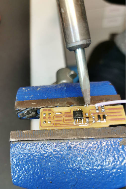
5.B.3. Programming process
At this stage, I have followed the same tutorial as for the milling process. (Brian)
There it explains where to access the configuration of the programming environment in windows. Tutorial.
These are the steps to follow:
-
Install the Atmel GNU Toolchain
-
Install GNU Make
-
Install avrdude
-
Download Zadig
-
Update your PATH
-
Install Drivers for your Programmer
-
Sanity Check
After this, I continued with Brian’s tutorial, programming the in-circuit programmer using a mother programmer who left us from Fablab León to Álvaro and me so that we could do this assignment.
I follow this programming tutorial
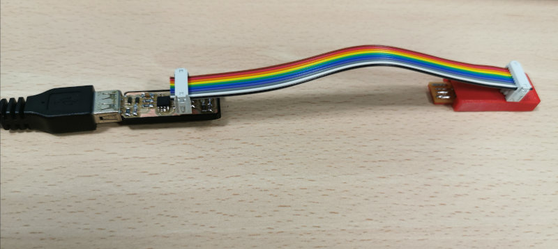
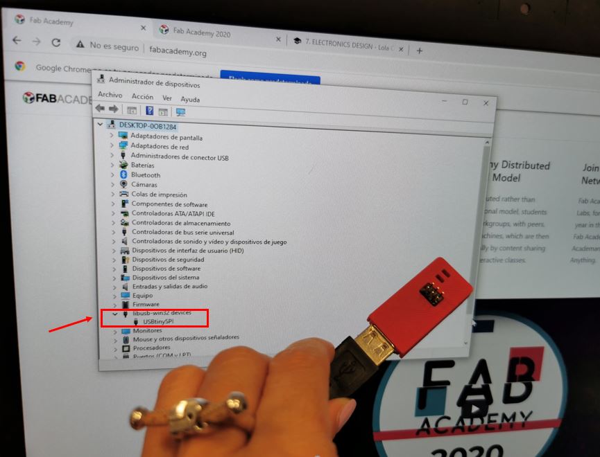
I check that my FabISP is recognized by my computer.
Then I used a Hello Board to test my programmer.
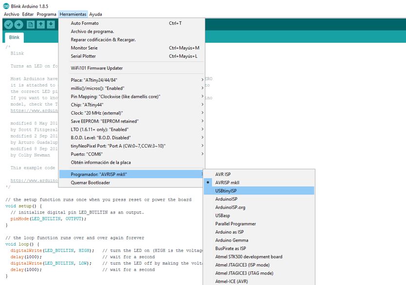
For this we have used the Arduino IDE software. To start we have configured it to program the ATiny45 boards.
We have used the example sketch “Blink” to program the Hello Board.
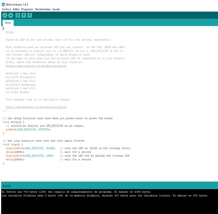
It didn’t work so we had to check wires, connections, programmers, and although from Arduino IDE, everything was correct, we couldn’t get the green LED of the Hello Board to flash.
With the help of our colleagues in León we discovered the fault. We had not changed the LED pin. We put 7 and it was the right value that made our Hello Board work.
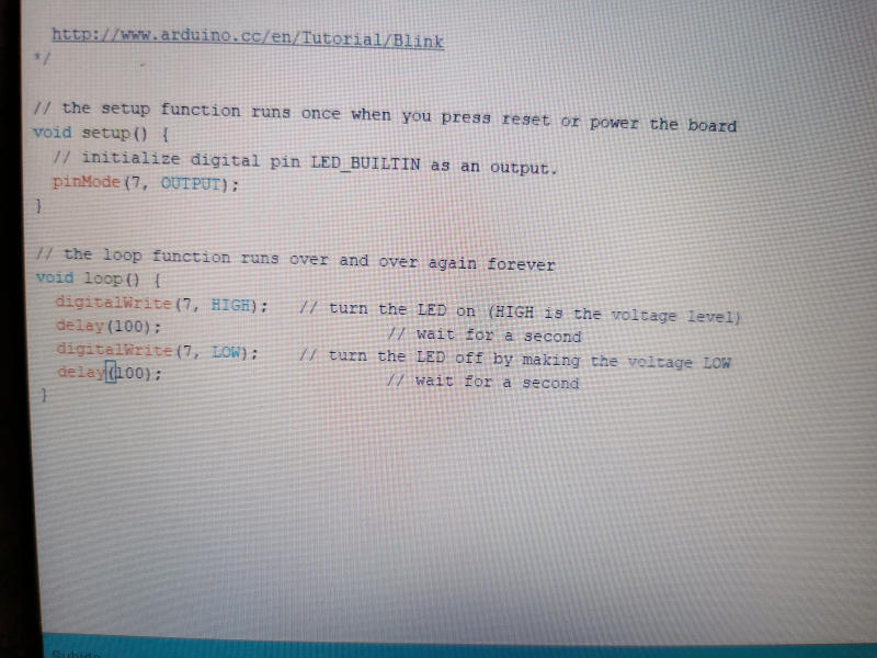
Also adjust the delay between turning the LED on and off.
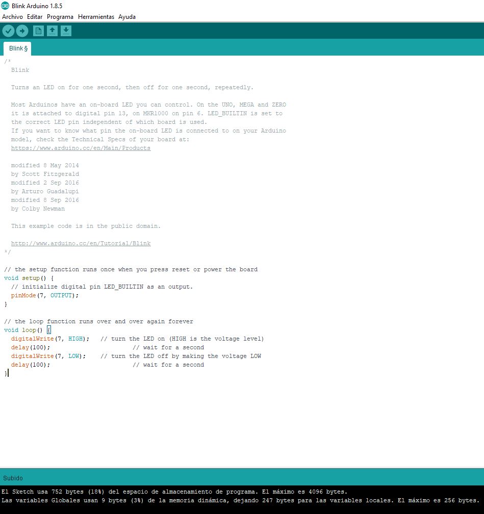
This is what happens now:
Wow! My nightmare had a happy ending.