7. ELECTRONICS DESIGN
-
Group assignmet:
- Use the test equipment in your lab to observe the operation of a microcontroller circuit board.
-
Individual assigments:
-
Redraw an echo hello-world board, add (at least) a button and LED (with current-limiting resistor).
-
Check the design rules, make it, and test it.
-
Extra credit: simulate its operation.
-
I have continued using my weekly planning in which I have updated my activity in FabAcademy
This week, after participating in the 3D printing and scanning review, which are fields I usually work in, after Wednesday’s Lecture on electronic design, I was highly motivated to do a good assignment and be able to document it correctly.
So on Thursday, Friday, Saturday, and Sunday I spent them thoroughly learning electronics concepts and learning to design my own boards.
But over the weekend I started to feel ill, and on Monday the 9th I had to undergo emergency medical intervention. I spent two days in bed and the doctor gave me medical leave at work. I have a very strong work rhythm and now with FabAcademy I have no life. I need to rest. My body warns me.
So this week I have gone as far as I can and the documentation will be updated step by step.
I joined the Lecture on Wednesday of Computer Controlled Machining and try to continue with great interest, but low energy and poor health.
7.A. GROUP ASSIGNMENT
The Group Assignment page is at the following link.
As in previous assignmemts, this week I made the group assignment with my co-worker Álvaro Macián, we are both from Sedicupct-Fablab and our local Fabacademy node is FabLab León.
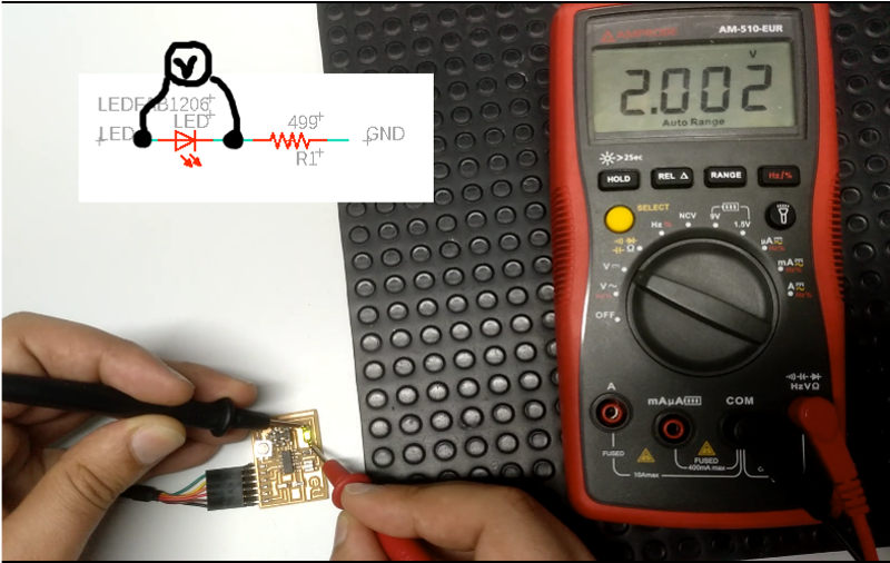
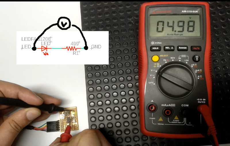
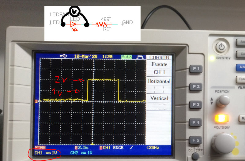
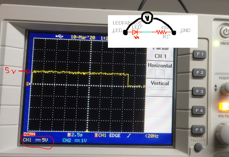
We have used a multimeter and an oscilloscope to measure the voltage in the elements of a hello board. Previously we have loaded the blink program which makes the board led flash. To measure the voltage drop of a component, the tool with which we are going to measure it must be placed parallel to it.
We select the option to measure DC voltage. And we measure the voltage drop in the LED and also in the resistance that is connected in series with the LED. The sum of both must be equal to 5v (voltage of the output pins of the microcontroller).
- Multimeter
- Oscilloscope
-
Results
V (led) = 2v
V (led + R) = 5v
V(R) = 3v
7.B. INDIVIDUAL ASSIGNMENT
To carry out my individual assignment that consists of designing my own board Hello Board , I have been guided in this Tutorial of the software Eagle that I have used to configure my design.
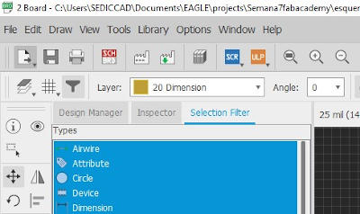
7.B.1. Libraries into Eagle
To do this, the first thing I have to do is download the Fab Libraries and make them available in Eagle.
To activate the electronic library, from Eagle you have to right-click and import them, accessing “Open library manager”.
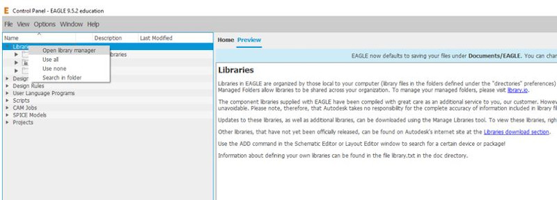
From here the Eagle libraries are imported from the Fabacademy link
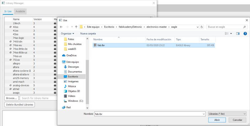
Also, from “browse” you reach the file fab.lbr which is the library of the electronic components that is in fabacademy.
It does not appear in the list of available libraries, I will see how I can solve it. Possibly closing and opening the program ?, I’m going to try…
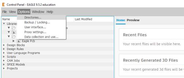
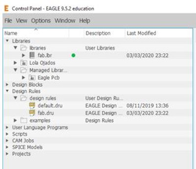
It has not worked, so from “Options” I can see the directories where the Eagle libraries and the design rules are , here I am going to find the library that I need.
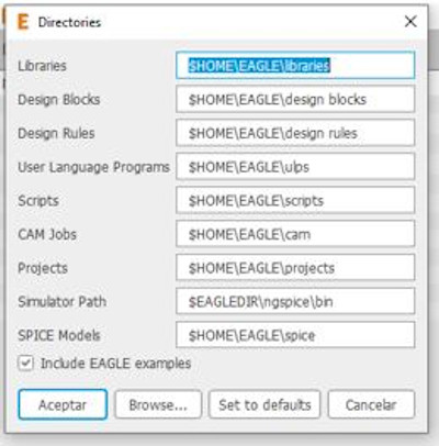
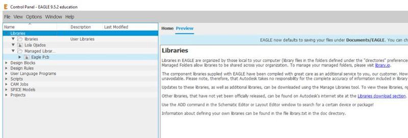
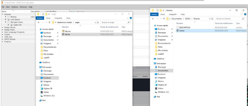
When Eagle was installed, a folder was created in Documents on my PC. This is where I will paste the files from the Fabacademy libraries and design rules.
I copy the .lbr file into the libraries folder
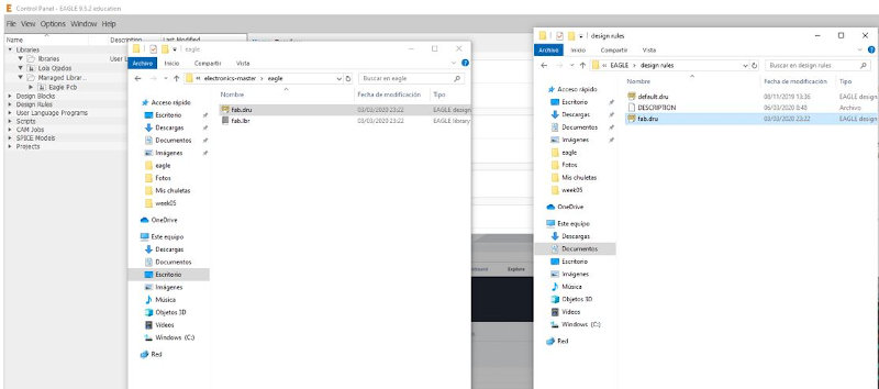
I also copy the design rules in their corresponding folder
Now I already have both files active in Eagle.
Make sure that the circle next to the library is green , which means that it is active , if it is not, press and activate it to access the components here.
From here, I can start to design the PCB
7.B.2. Design of my PCB
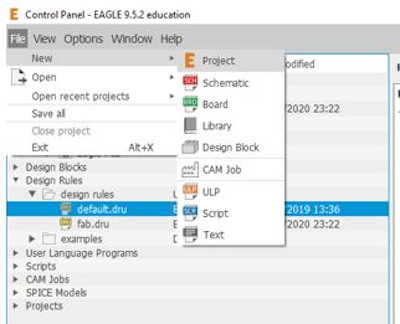
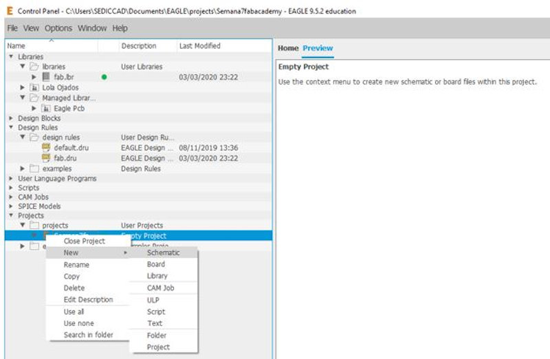
With file - New Project access to the board design interface:
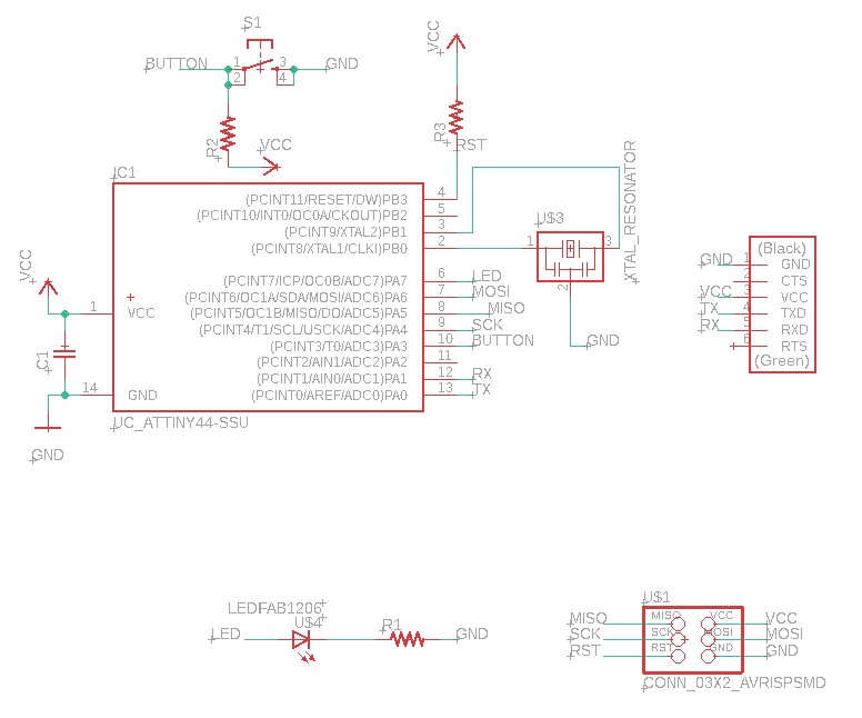
First, the circuit is configured in a “Schematic” way for its initial design, and from this scheme the components can be distributed and placed on the board itself so that the tracks do not cross and everything is well configured.
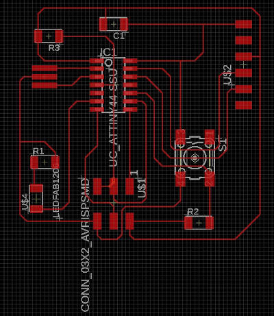
The board that according to this week’s assignment must be manufactured and programmed is a “Hello” type and the microprocessor to be used is the ATtiny 44.
The result will be this:
This is the link where I have followed the Eagle tutorial to make this board.
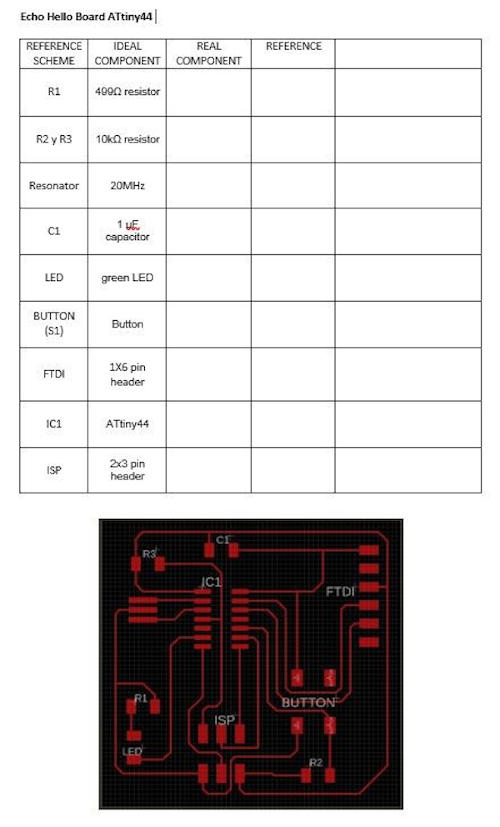
Components
These are the components that I need to make the “Echo Hello Board”.
Parts Already on the Hello Echo Board:
• 6-pin programming header: for programming the board.
• Mmicrocontroller: attiny44A. Once the microcontroller is programmed, the program stored in non-volatile memory. This means that it will remember the program.
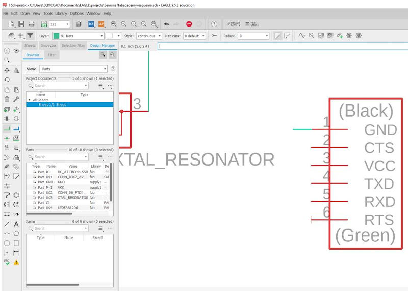
• FTDI header: powers the board and allows board to talk to computer.
• 20MHz resonator: external clock. The attiny has a 8Mhz clock but the resonator is faster (increase the clock speed of the processor) and more accurate.
At a minimum you should add the following components to the schematic:
• Resistor (value 10k ohms) Purpose: pull-up resistor.
• Button.
• Ground.
• VCC.
• Connector pin 10 (PA3) on the micro-controller to the button.
• LED (Light Emitting Diode) (LEDs have polarity - the side with the line is the cathode and connects to the ground side).
• Resistor (value 499 ohms) Purpose: current limiting resistor. (Why do we need a current limiting resistor? So we don’t burn out the LED).
• Resistor (value 10k ohms) Because, the LEDs we are using are rated for the typical forward voltage is between 1.2-2.2V, so, we need to use a 82 ohm resistor or above to avoid blowing out the LED. I chose to use a 10k ohm resistor, but you could use other value.
Design
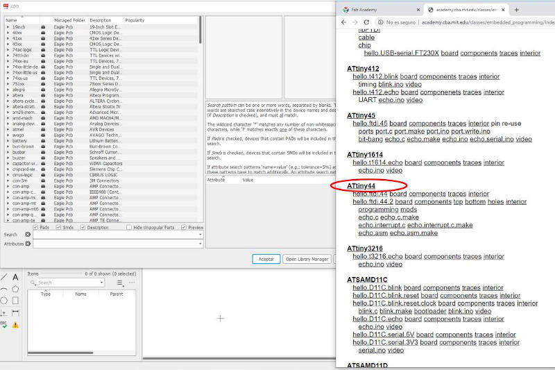
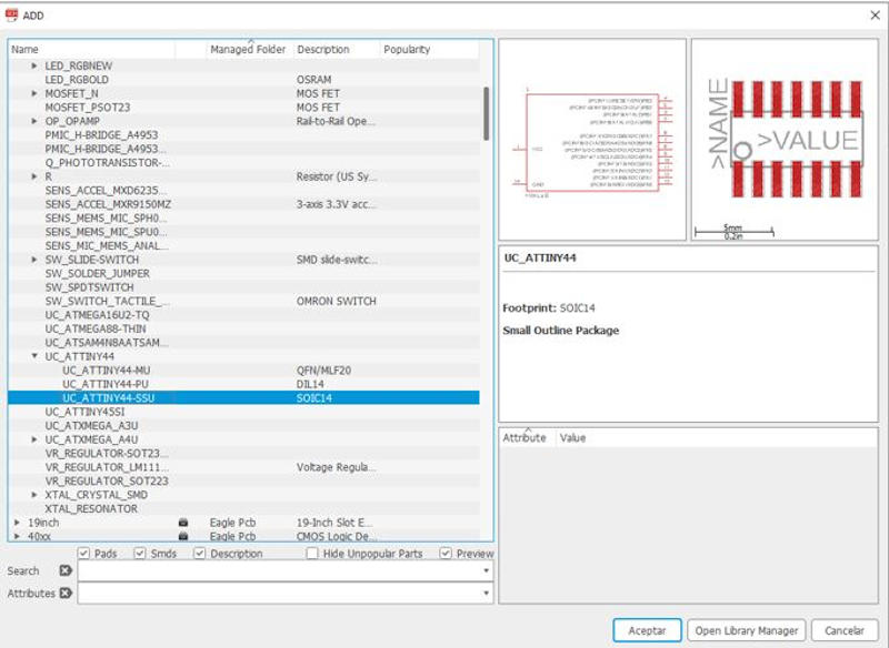
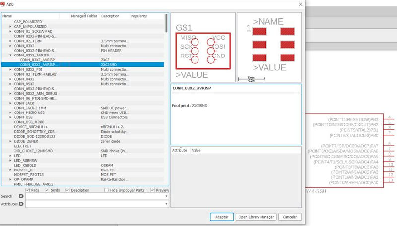
From Eagle, in the schematic window, I look for the fab library and there its components:
First I find and insert the ATtiny44 microcontroller.
Then the 6 pin connector (AVRISP)
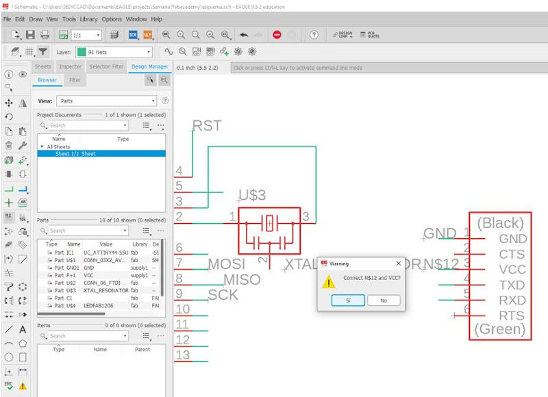
After introducing all the components, I introduce the connection cables, and in other cases I put labels that will serve to connect some terminals (pins) with others.
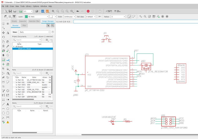
Cables
Labels
The label is inserted at the end point of the cable and with the right mouse button you access the option to change its name (name), indicating the name of the terminal to which you want to connect.
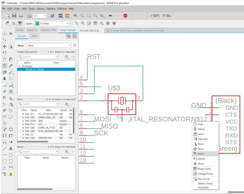
When it is indicated a terminal to connect the label that we are entering, the program asks if we want to make the connection, we will say yes.
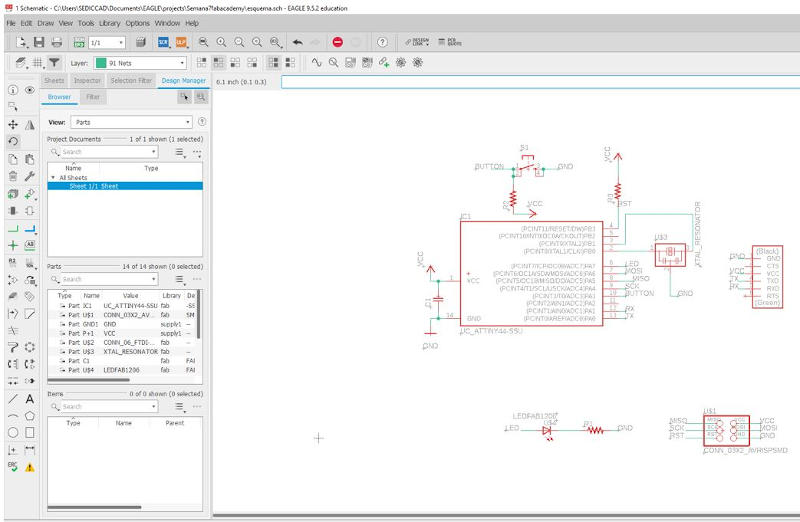
After configuring all the components and putting all the connections, this is how my scheme is:
Now comes the complicated, at least for me …
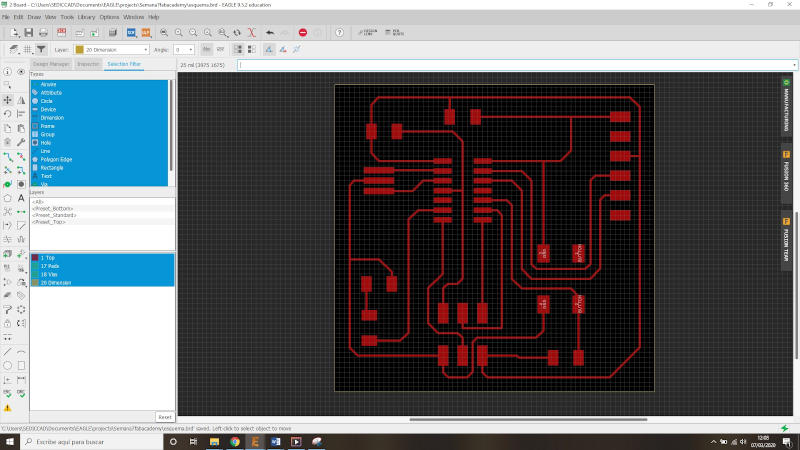
I go to the window “Board” (I leave the Schematic) of the Eagle program.
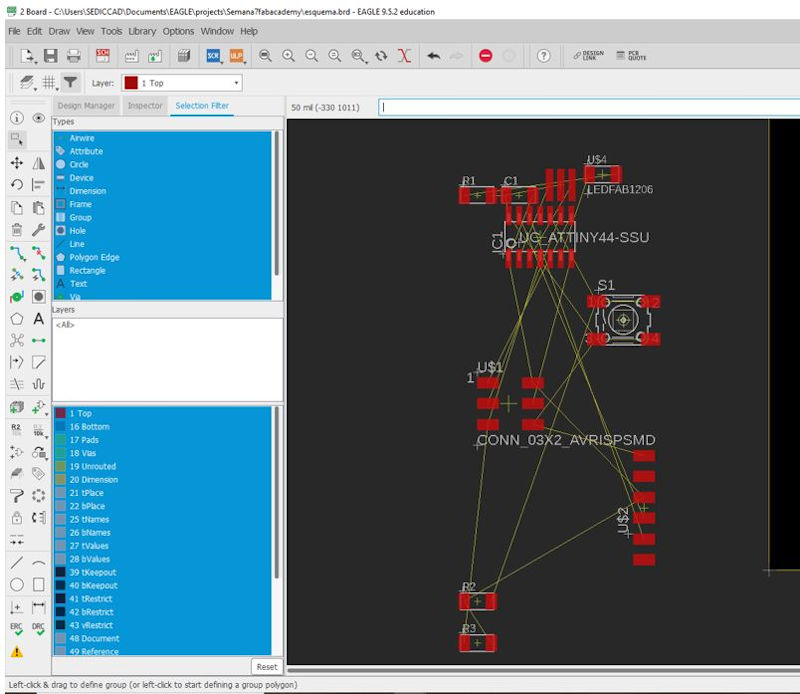
I place all the elements within the space that the plate symbolizes, more or less ordered and proceed to draw the tracks that will then be milled on the plate.
I have to be very careful and patient.
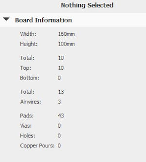
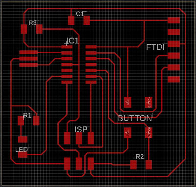
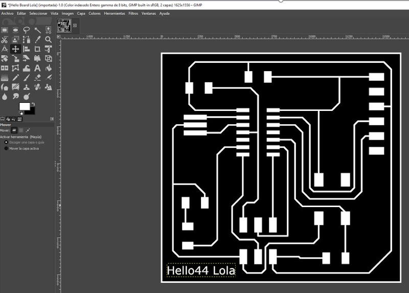
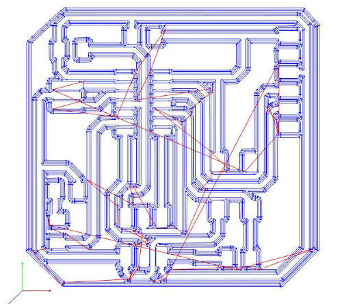
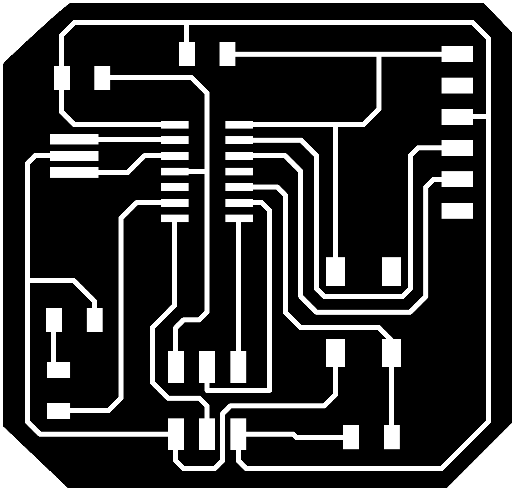
After a long time playing to find ways of union between the components, I manage to have everything connected and the circuits configured and the result of the design of my board is this:
The tutorial that I have followed and to which I have previously referred, indicating its access link, contains indications about the design rules that I have not yet followed, specifically these types of things were indicated:
Design rules check
After designing our board we need to check that the endmill we are using is able to go between all the traces so the machine is able to cut successfully the board. For that we are going to use Design Rules Check (script) that will check that there is enought space everywhere.
To do this, you can follow these steps:
• Download the DRC script from here
• Type in EagleCad drc and press enter.
• A new dialog box should appear where you can LOAD the script.
• If everything is correct no error messages should appear.
• In case some red areas appear between the traces, you should move the traces leaving more space between them.
Tips and Tricks
• In free version of eagle, don’t put anything below or to the left of the cross (origin) in either schematic or layout.
• 0 ohm resistor trick: place a 0 ohm resistor over a trace to hop over an existing trace.
• Junction (symbol is a dot) can be useful when a net splits into two different nets - indicates whether two nets that crossover are connected or not…
• Under options you can change the background colour of the schematic/layout (User Interfaces)
• Click on display to see the layers which you can show/hide.
• Layout pieces in Layout - use right-click to rotate components.
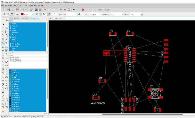
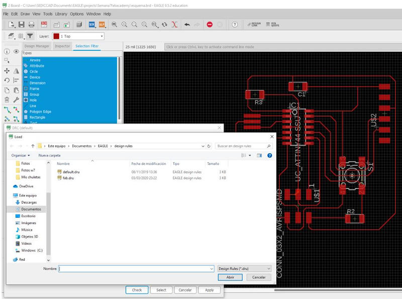
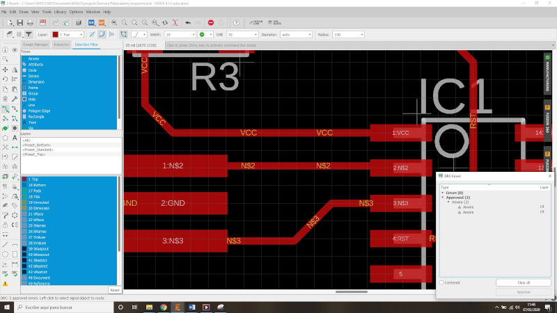
Since I didn’t do it before, now I have to load the design rules for it, I have to access DRC and Load.
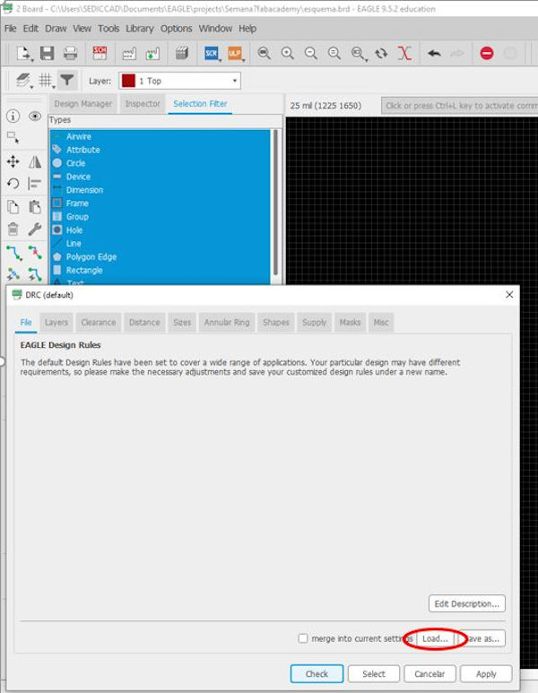
I select fab.dru and then “Open_Apply”
And then you have to do a “check” to see if I have complied with the design rules.
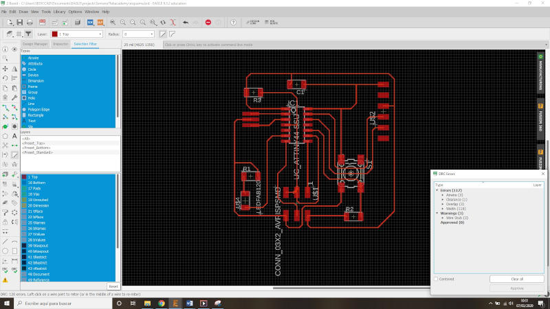
Horror!!!
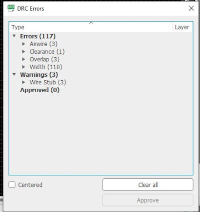
I get more than a hundred errors, and most have to do with the thickness of the circuit lines that I set by default, are too thin.
In my ignorance I thought that:
What appeared in my design was later easily configurable and then when sending to mill the thickness or thickness could be changed … But I was very confident in my good destiny !!!
Now I have to change thicknesses and I don’t know if there is a way to change them all at once or I have to go one by one …
I’ll investigate.
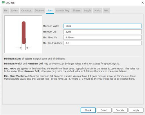
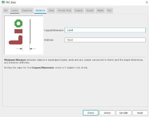
These are the rules that I have to follow and it is not like this.
I ask my classmates and instructors and they also indicate that we have to have this distance fixed as a design rule.
We do this because it has not given us errors of this type. Track width only.
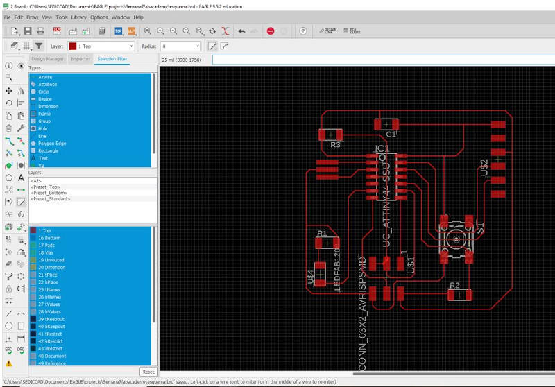
So I proceed to change the track width of my already configured board layout one by one.
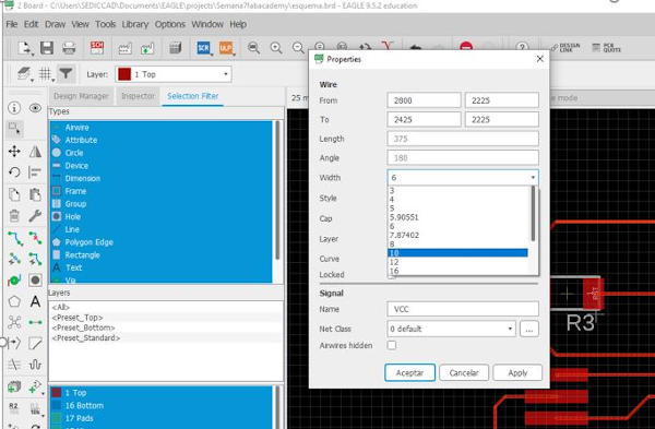
Change from 6 which is by default to 10. In “properties” that appear by right-clicking on each track.
Another option is to erase the tracks and draw them again.
I opt in principle to change properties and in some cases it is simple, I will erase and redraw. But either does carry the same runtime.
This is what should have been configured at first, if I had been more savvy.
I have found an internet forum and I have tried to put in command line:
“Change width 10 mil”
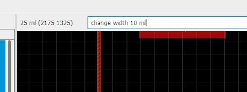
Executing this lets me select each cable that I want to change and sets it to 10mm thickness, at least I don’t have to click the right button_properties_change from 6 to 10 for each of the selections.
Ideally, this would allow me to select all objects and change them at once, but, something is something…
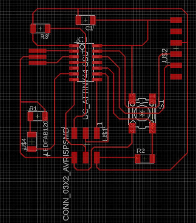
This is my board with all tracks changed to 10mm.
I’m going to do a check
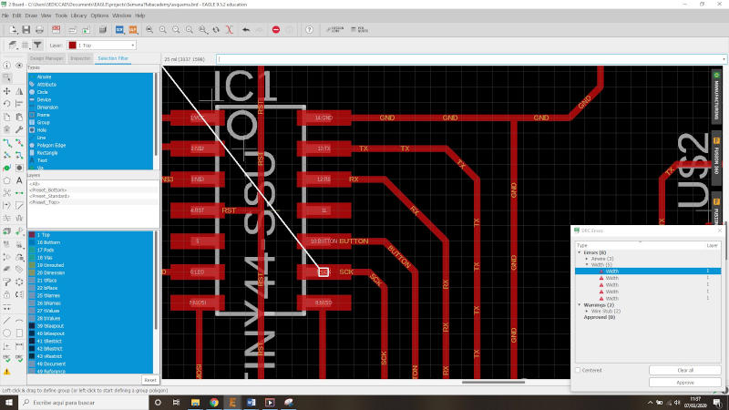
There are still a few small errors that I am correcting, especially at the ends of the tracks under the components.
I finally solve all the errors. Yuhu !!
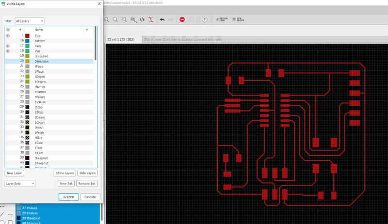
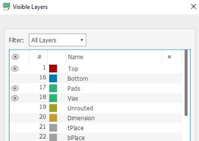
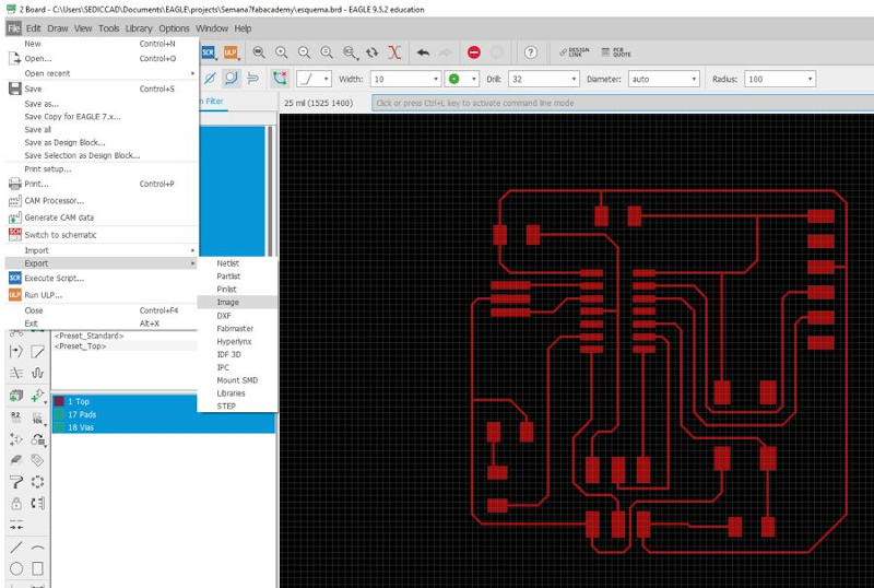
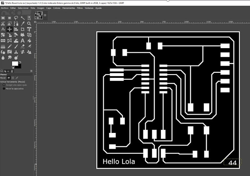
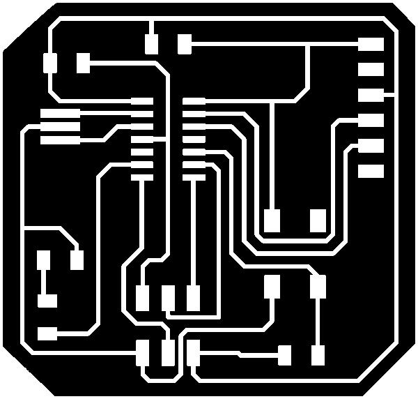
To prepare the board for milling, I must leave only the layers to be machined visible. And they are (Top, Pads and Vias):
I export image,
But before that, I’m going to adjust the size of the base to print the circuit on. Or what is the same to adjust its dimensions to the designed circuit.
I put the “20 Dimension” layer (in which the plate dimension is drawn) as current, activate the “selection filter” tab and with the move command, adjust the dimensions.
I continue with the export process:
I put the parameters recommended by my instructor Nuria:
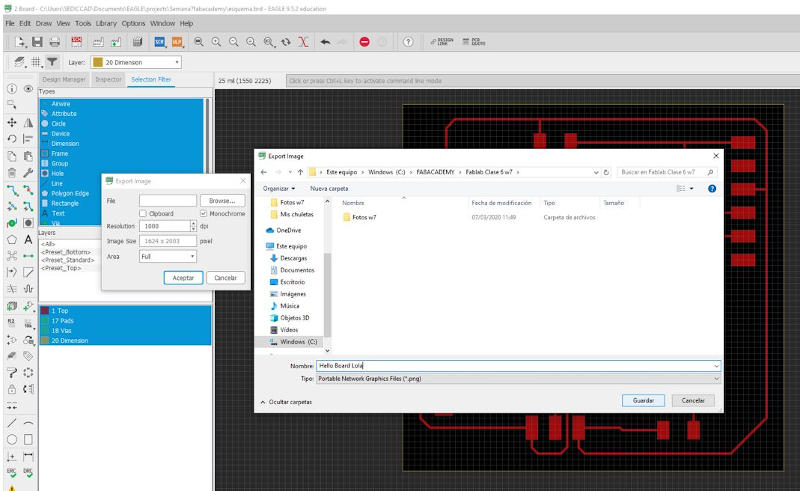
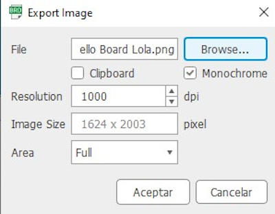
I save as .png image (default format) in the folder of my choice.
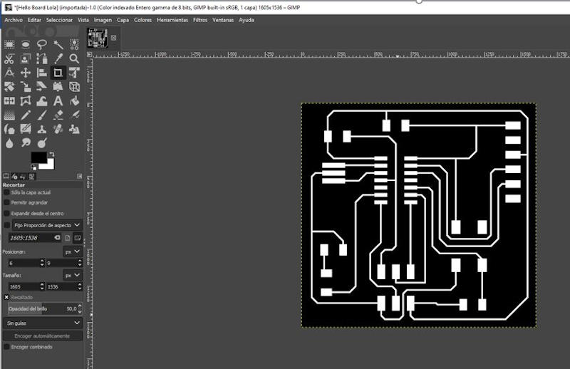
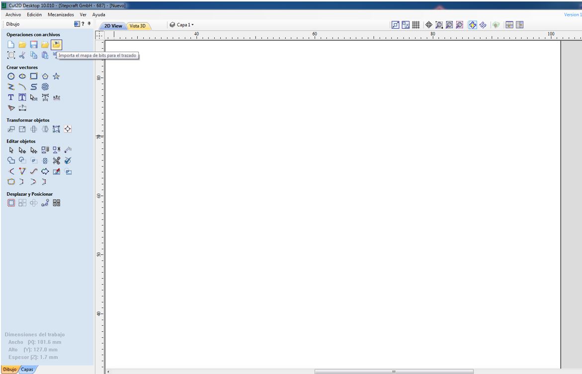
The exported image, I open it with GIMP
In GIMP, I resize with a crop and the image looks like this:
I continue with the tutorial:
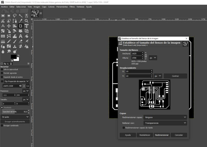
Change canvas size by increasing 20 pixels to the height and width of the image and the center.
Use “flatten image”
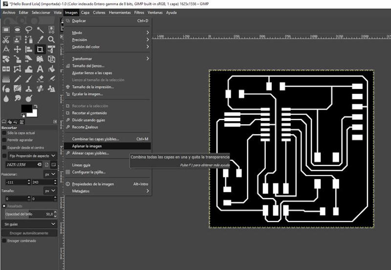
So is my board:
I export it as Hello Board Lola rev.png
Now comes another drawback: I don’t know if I have the scale image. This obstacle will have to be overcome and I will have to figure it out.
I check the scale in the mill program where the GCODE is generated. The CUT2D where the image is imported has a tool to measure, I measure the distances of my circuit and thickness and I check that it is at 1: 1 scale.
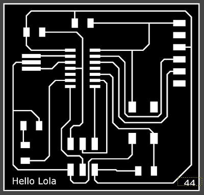
Now I also have to make the external image to cut the plate on which I am going to print the circuit. I use the one I have, I export it from GIMP as png with this other name:
Hello Board Lola rev1.png
And fill in black with the tool fill in everything that is part of the circuit except the outer line that delimits the edge of the plate.
When finished I will export it again, but with the name Hello Board Lola rev2.png, just in case …
Now I have:
I make a sheet to put the components and solder them later.
In this document I have an adhesive and I put the different components each in their place, they are very small and this helps me to have them in order and that they do not get lost while I take them and weld them one by one.
I follow the corresponding document process accessible at this link.
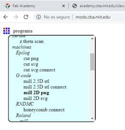
In the browser: mods mit_left button programs_open server programs_G-code_mil 2D png
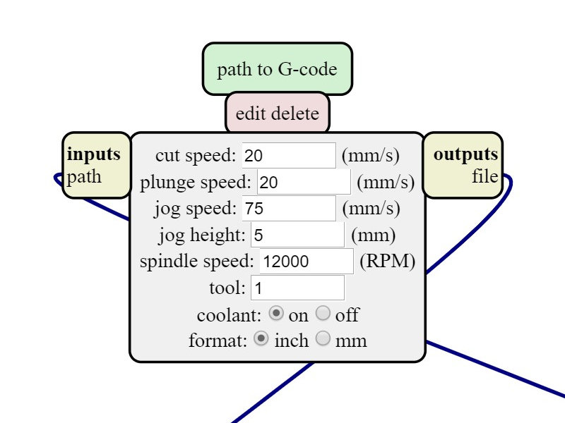
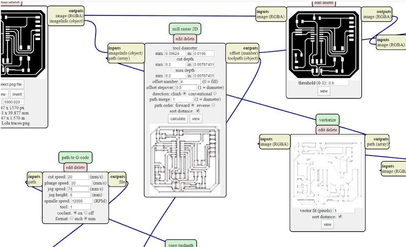
I proceed to Calculate
7.B.3. Milling process
I’m going to the Stepcraft 420 milling machine
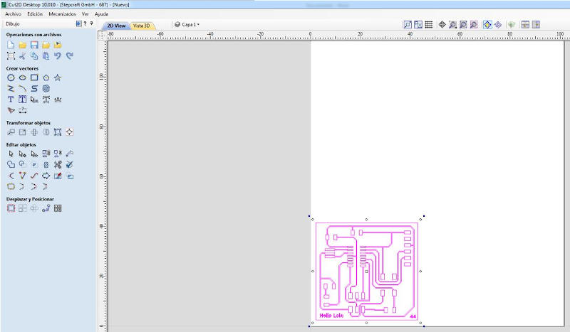
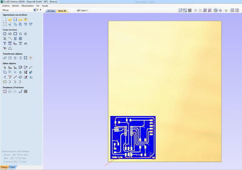
For the milling process, I import the images from CUT2D Software
The image of the designed and exported electronic board is vectorized
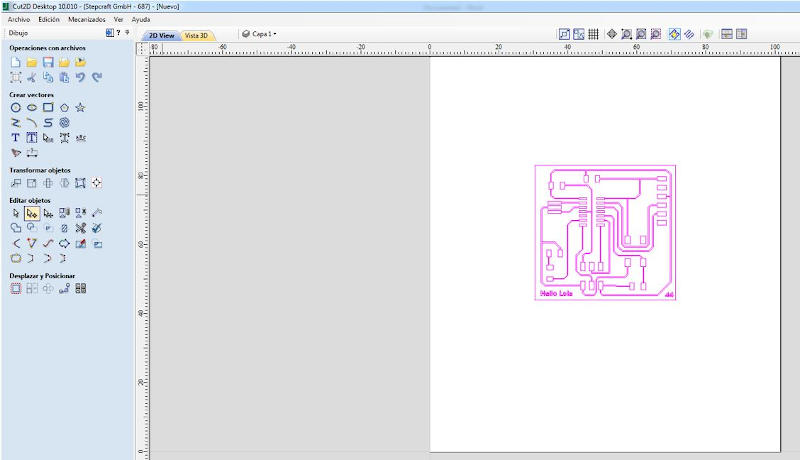
I position the vectorized image on the edge of the board to optimize space and save material
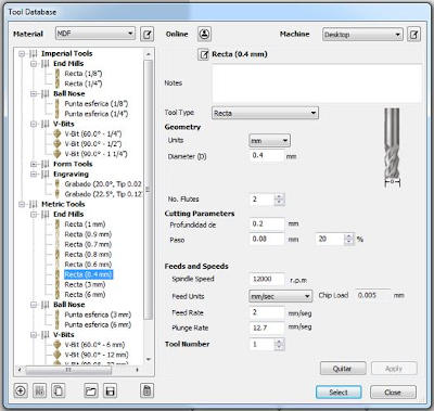
I perform the pocket operation by selecting the 0.4mm straight tool
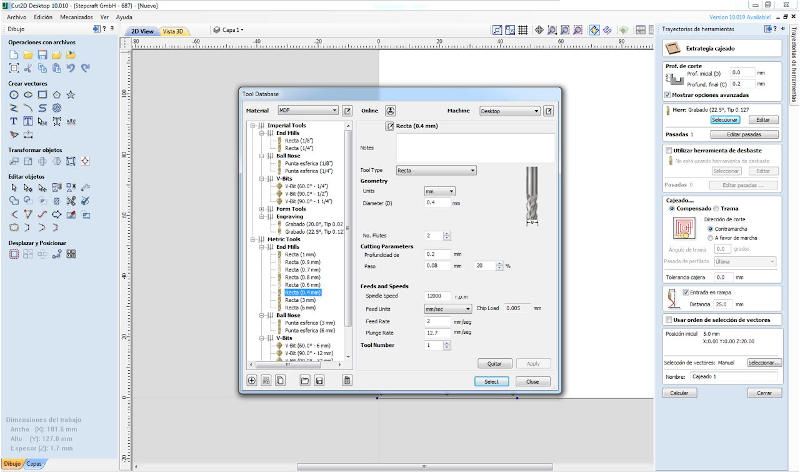
I save the generated file and name it “Hello Lola traces”
In the step craft software of the milling machine
The GCODE created from CUT2D is opened and the x, y and z coordinate system of the mill is configured
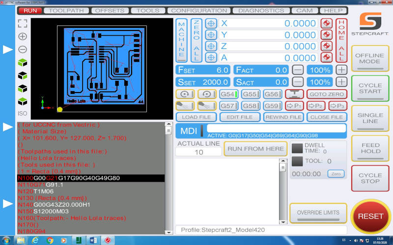
I click on “Cycle Start” and the mill starts with the milling process.
It will take about 2h.
My circuit milling machine is already milling!!
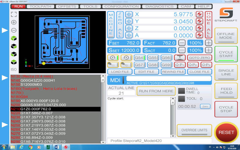
Another beginner problem
While my board is being milled, I check that the tracks are still very thin and some of them have been interrupted and broken because the mill has roughened more than it should and has not turned out well, those that are still visible, are too fragile, so I stop the milling process and decide to do it again by modifying the thickness of the lines that make up the copper tracks.
So I go back to my “Eagle” design and with the same command that I found in the forum (“Change width 12 mil”) I make my tracks wider, I put the value of 12 mil instead of 10 mil.
I go through the process of exporting my board again and prepare it to mill now with these new features, and the result, now, will help me to solder my components and get my own Hello Board.
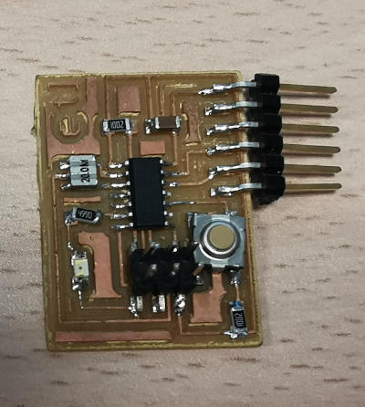
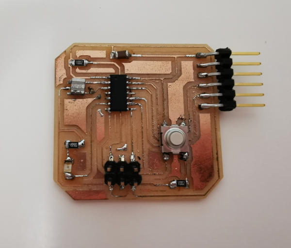
The milling result of my circuit board is this:
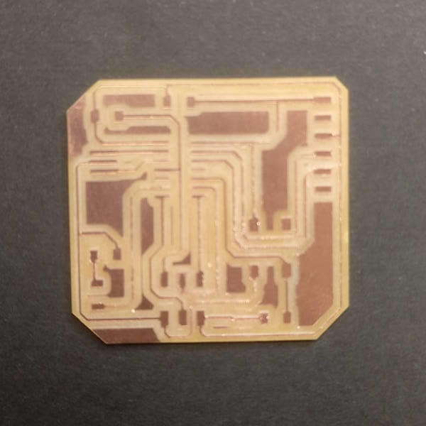
Even having changed the thickness of the tracks to 12mil, I think they are very thin, possibly it has to do with my type of milling machine, or with the tool I am using, so in subsequent designs I will use a width of 16mil better.
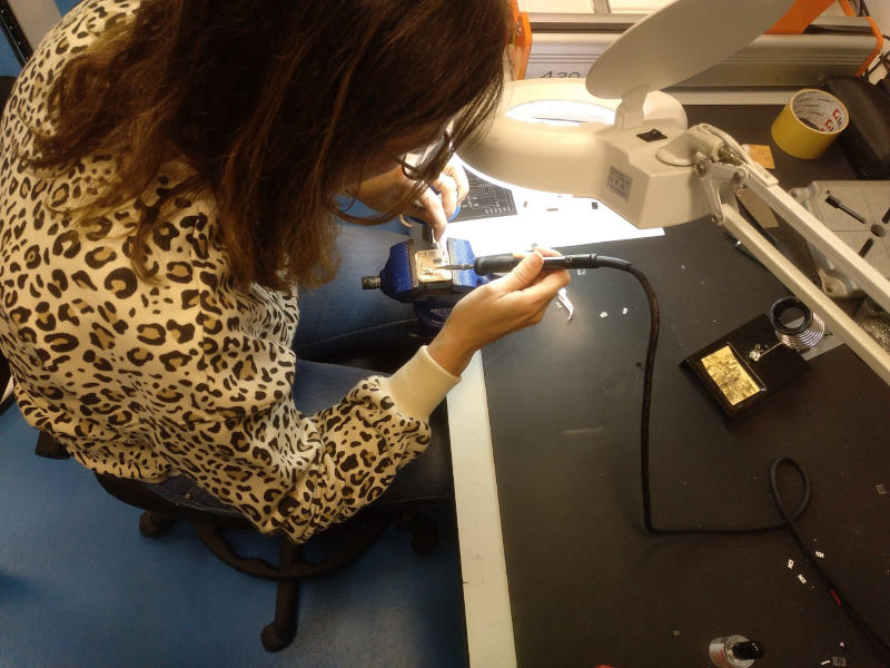
7.B.4. Welding process
The next thing I have to do is solder the components to the board, for that the table that I have already shown before along with the scheme of my board helps me.
I start to weld,
I need a 2-row 3-pin ISP connector, which I don’t have now, so my colleague Álvaro teaches me how to fix it.
Using two 1-row, 3-pin connectors, I put them together in the flat cable connection and I know how I have to glue them together.
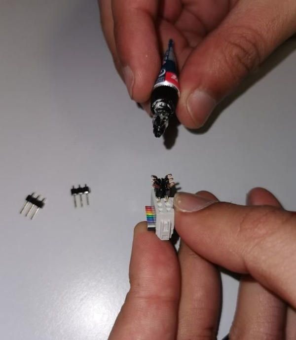
So, I can continue to weld
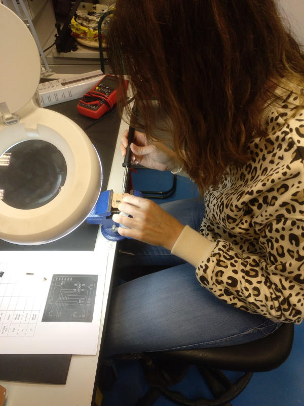
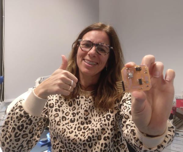
And when I’m done, my board is just as pretty.
7.B.5. Programming
Now I have to face the next challenge.
For me, getting these things done with electronics is quite an achievement.
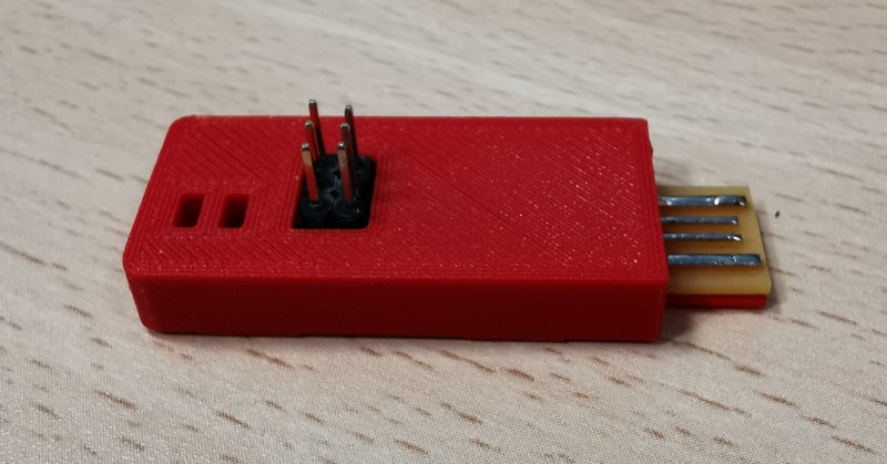
To program my Hello Board, I use the programmer I made from Brian’s tutorial in week 5: electronics production and the Arduino IDE software.
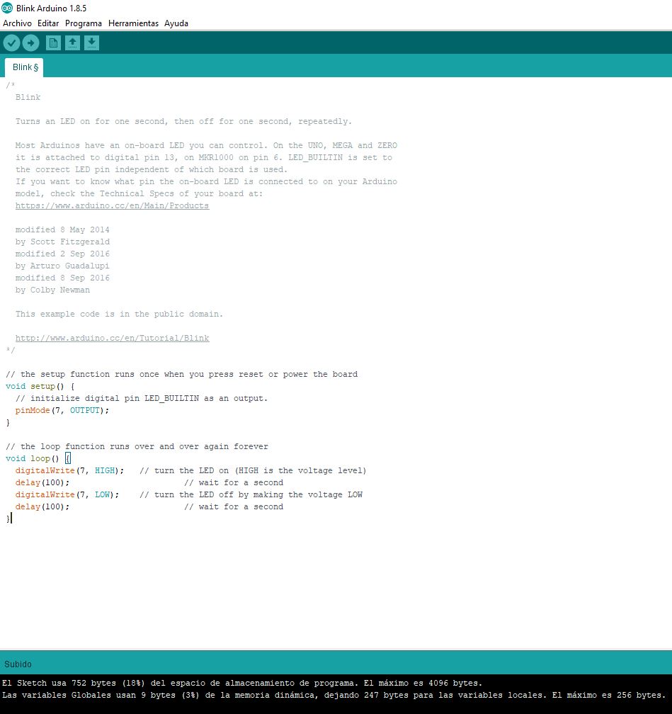
From here, I have tested the blink programming code that I used to check the working of the programmer that I replicated in the week 5 assignment.
I make the necessary connections this way.
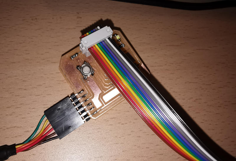
And the result has been this:
Works correctly!
And finally, I try to program my Hello Board with my own FabISP programmer that I made in the assignment of week 5.
This is the resault:
I am very happy to have achieved this, the electronics cost me especially because I have never studied it, nor practiced it, I have used elements already commercially available.
7.B.6. Files used for this assignment
- EAGLE file:
- Board PNG files:
- Arduino Code: