7. Electronics Design
-
Individual Assignment
- Redraw an echo hello-world board
- Add (at least) a button and LED (with current-limiting resistor)
- Check the Design Rules
- Make it!
- Test it
- Extra credit: simulate its operation
-
Group Assignment:
- Use the test equipment in your lab to observe the operation of a micro-controller circuit board
Research
PCB design software: Eagle
Assistant lecturer: Antti Mäntyniemi. He introduced the basics of PCB design and Eagle PCB design software.
Local Class, contains Tutorials
https://gitlab.fabcloud.org/academany/fabacademy/2020/labs/oulu/local/-/wikis/Classes/Electronics%20design
fab.lbr library for Eagle: contains components used which can be used for FabAcademy.
https://gitlab.cba.mit.edu/pub/libraries/-/tree/master/eagle
Schematics, as a starting point for redrawing an echo hello-world board
http://academy.cba.mit.edu/classes/embedded_programming/t412/hello.t412.echo.png
SnapEDA: A Free PCB Footprints and Schematic Symbols
Not all required parts are in fab.lbr library.
Other required libraries/parts:
-
ATTINY412-SSF
https://www.snapeda.com/parts/ATTINY84A-SSF/Microchip/view-part/?ref=search&t=ATTINY412-SSF
-
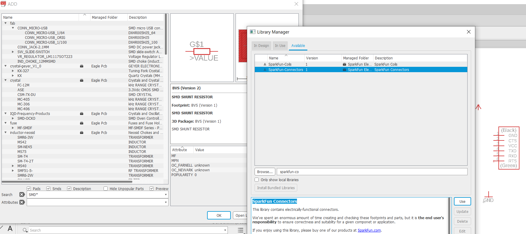
SparkFun Connectors Library.
Eagle
Adding Library to Eagle
Eagle Control Panel:
- Find the Directory for Libraries
- Options > Directories
- Copy the Library file into that directory
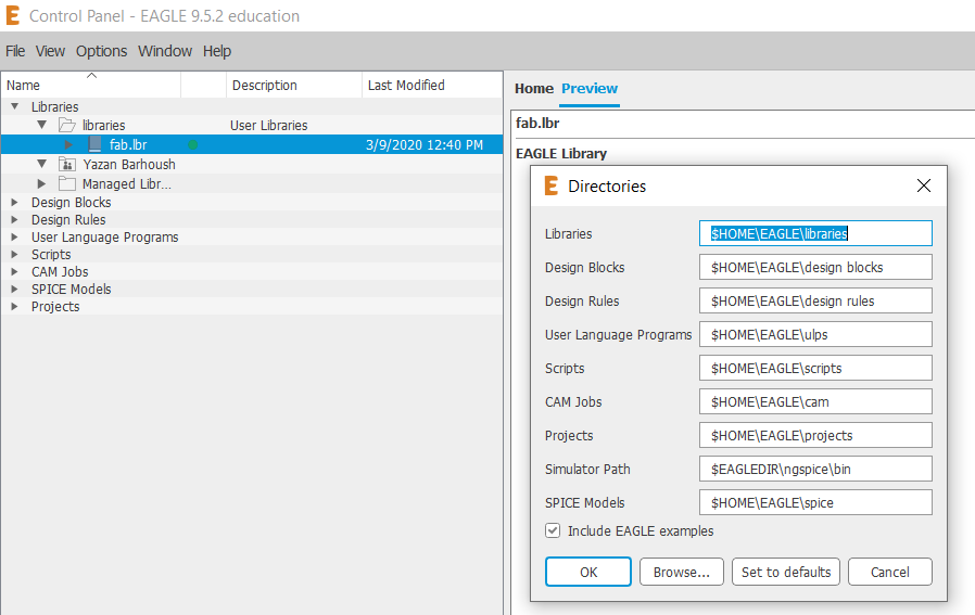
Library Manager can also be used to check if the library is in use!
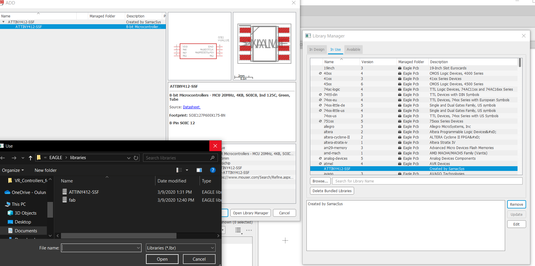
SparkFun Connectors Library can be installed using the Library Manager.
Schematics
Start a new Schematic:
Eagle Control Panel:
- File > New > Schematic
On Schematic, the following editor commands were used
ADD command
-
Function
- Add elements into a drawing.
- Add symbols into a device.
-
Mouse keys
- Center mirrors the part.
- Right rotates the part.
MOVE command
-
Function
- Moves objects.
-
Mouse keys
- Ctrl+Left selects an object at its origin or modifies it (see note).
- Shift+Left selects the whole polygon (see note).
- Ctrl+Right selects the group.
- Left&Drag immediately moves the object.
- Ctrl+Right&Drag immediately moves the group.
- Center mirrors the selected object or the group.
- Right rotates the selected object or the group.
- Shift+Right reverses the direction of rotating.
DELETE command
-
Function
- Deletes objects.
-
Mouse keys
- Shift+Left deletes higher level object.
- Ctrl+Left deletes a wire joint or a port.
- Ctrl+Right deletes the group.
NET command
-
Function
- Draws nets on a schematic.
-
Mouse keys
- Right changes the wire bend style (see SET Wire_Bend).
- Shift+Right reverses the direction of switching bend styles.
- Ctrl+Right toggles between corresponding bend styles.
ERC command
-
Function
- Electrical Rule Check.
Tools > ERC
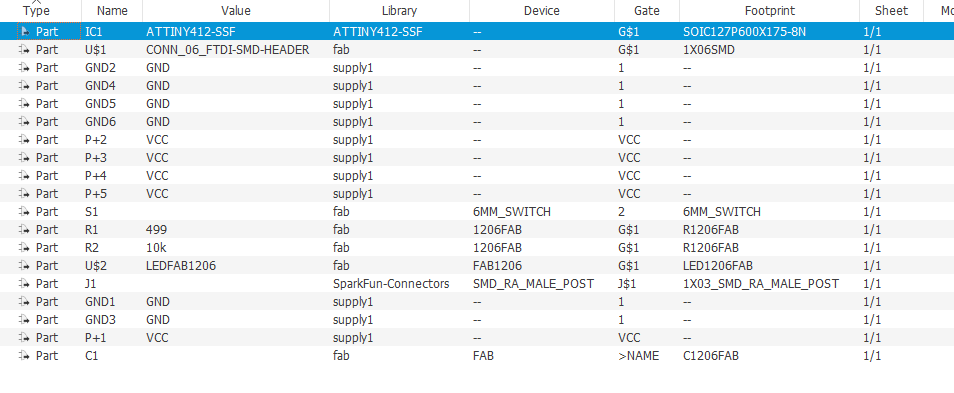
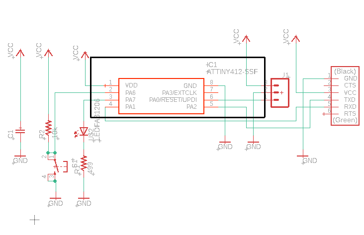
Figure below shows the list of required components.
A video showing adding, moving and netting components in order to build the schematic. ERC command was used to check electrical rules.
Figure below shows the final schematic.
Board
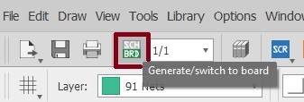
- Generate/Switch to board
- Rearrange components using the MOVE command.
- Use RATSNEST command to calculate shortest path.
-
Draw routed wires using ROUTE command.
- Set the width to 16mil.
- Make sure that you are on the Top layer.

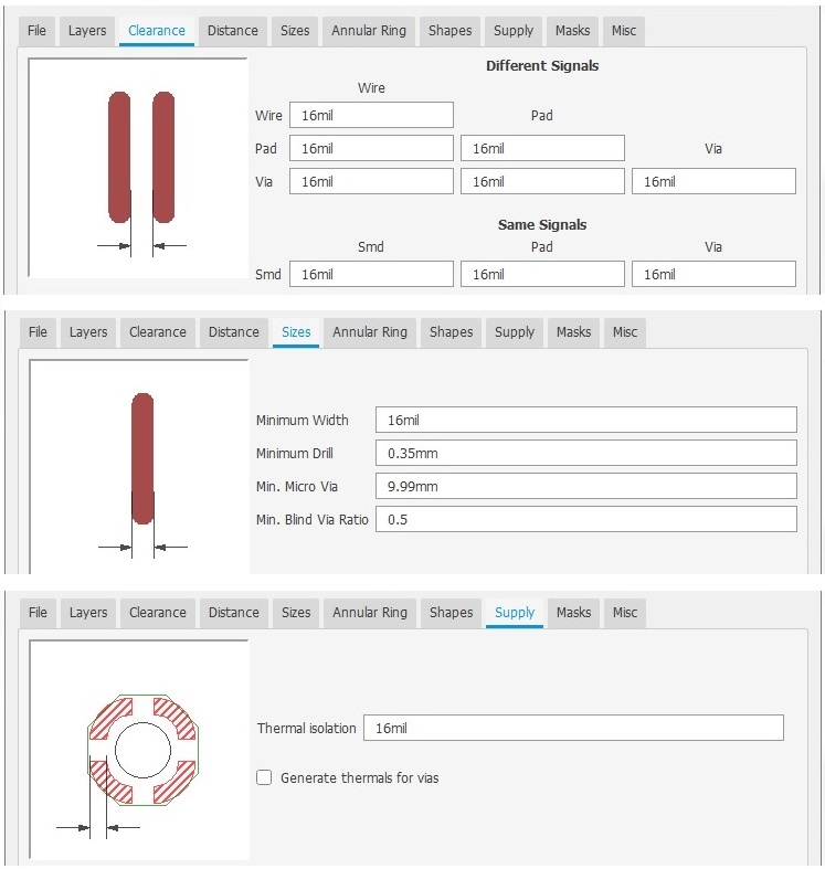
- Use DRC command to checks design rules.
-
Modify the size of the board
- Dimension layer (Layer 20)
-
Use DIMENSION command to check design dimensions.
- save some space for the 6 Pin header positioning.
-
Use POLYGON command to connect Ground:
- Select Top Layer.
- Select POLYGON and draw.
- A POLYGON with a dashed line will appear.
- Connect the polygon to ground by naming the polygon GND.
- Click on RATSNEST.
A Video showing the board modifications.
The commands used and results are explained below:
RATSNEST command
-
Function
- Calculates the shortest possible air-wires and polygons.
ROUTE command
-
Function
- Converts un-routed connections into routed wires (tracks).
-
Mouse keys
- Left starts routing from any given point along a pad, via, wire, or air-wire -OR* commits currently displayed intermediate route segments (and via, if layer changed).
- Shift+Left starts routing with the same width as an existing wire -OR* places a via and continues routing on the same layer.
- Center selects the next routing layer (and initiates via placement).
- Shift+Center presents start layer selection dialog when starting from a multi-layer object.
- Right toggles left/right direction of current bend styles.
- Shift+Right cycles to the previous wire bend style.
- Ctrl+Right cycles to the next wire bend style (see SET Wire_Bend).
DIMENSION command
-
Function
- Adds dimensioning to a drawing.
-
Mouse keys
- Center selects the layer.
- Right changes the dtype.
- Shift+Right reverses the direction of changing the dtype.
- Ctrl+Left when starting/ending a dimension does not select an object.
POLYGON command
-
Function
- Draws polygon areas.
-
Mouse keys
- Center selects the layer.
- Right changes the wire bend style (see SET Wire_Bend).
- Shift+Right reverses the direction of switching bend styles.
- Ctrl+Right toggles between corresponding bend styles.
- Ctrl+Left when placing a wire end point defines arc radius.
- Left twice at the same point closes the polygon.
DRC command
-
Function
- Checks design rules.
Tools > DRC
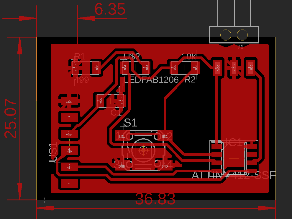
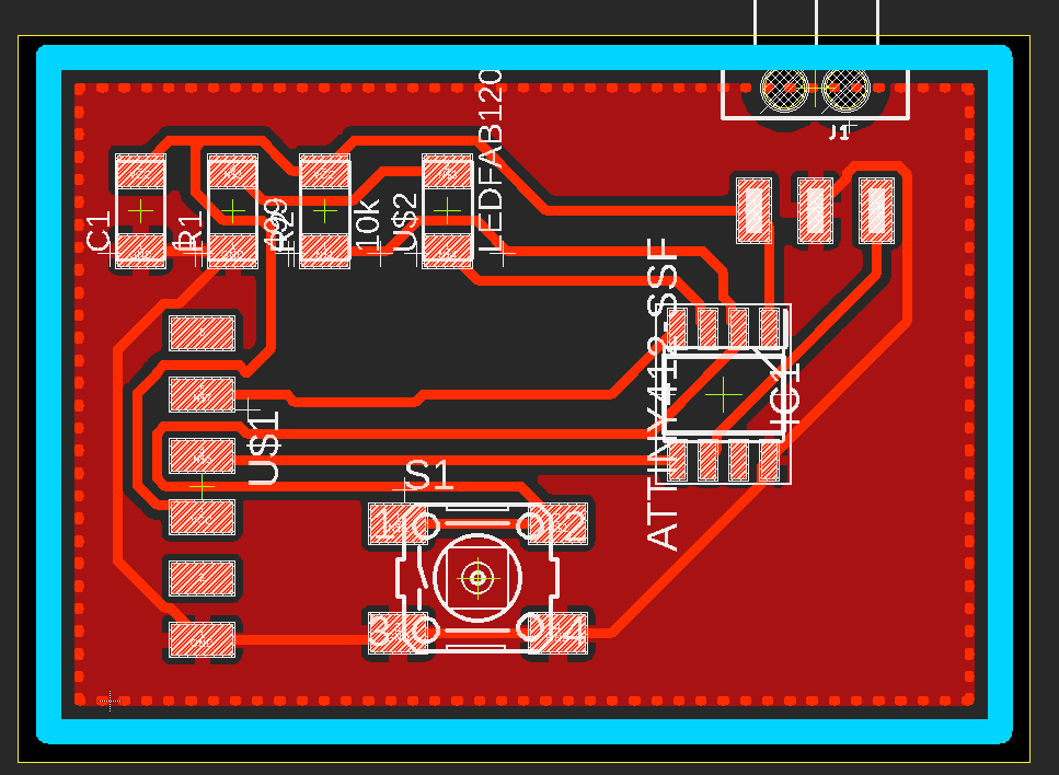
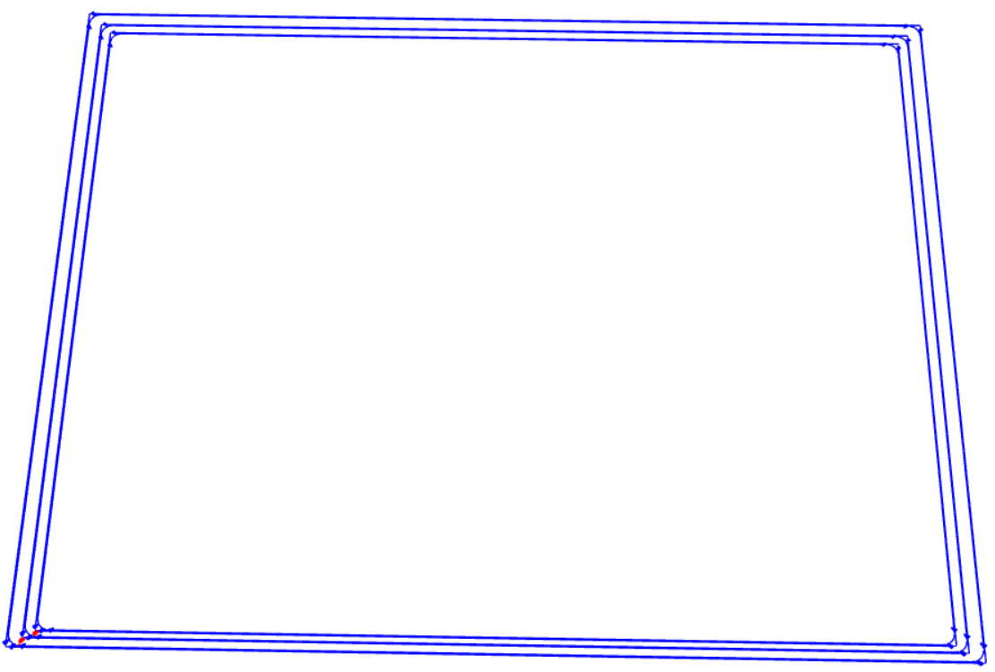
The final PCB outline, after connecting the ground properly.
Outline
- Set Layer to Milling (layer 46).
- Draw the outline using Line command.
Outline must be thicker than the diameter of the milling tool Therefore, for a 1mm milling bit, outline width can be 40mil (=1.016mm). We had to rearrange elements and do ground again.
Exporting
To export the traces:
- Set the background to black
option > User interface… > Layout > Background.
- Hide all the layers except the Top layer
View > Layer settings
- Export the image:
File > Export > Image.
- Set the resolution to 2400dpi and select the monochrome.
To export the outlines:
Same as steps as traces, except:
- Set Background to white.
- Milling layer (layer 46) visible only.
Milling
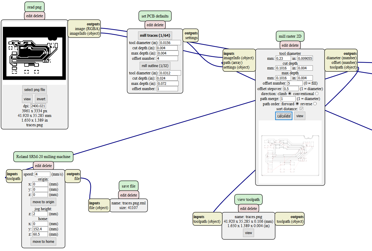
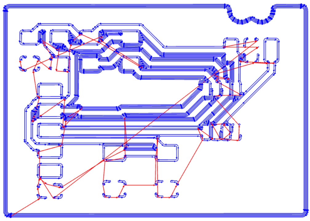
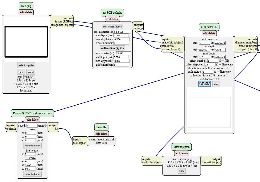
Producing .rml files
Using Mods Mods
Making an .rml file (Circuit tracing)
Making an .rml file (outline)
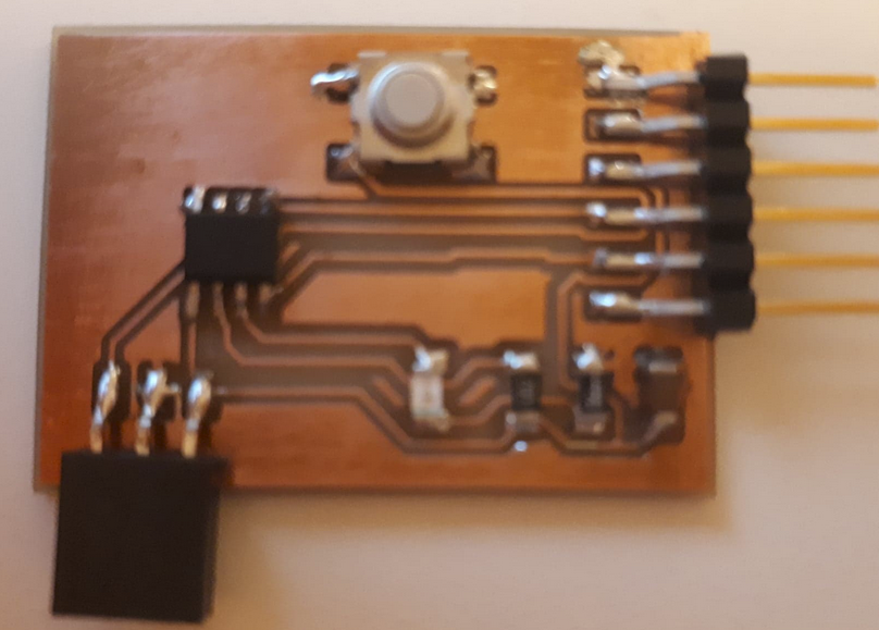
Soldering
Board Soldered
Programming and Testing
Using the programmer board fabricated in Week 4 Electronics Production
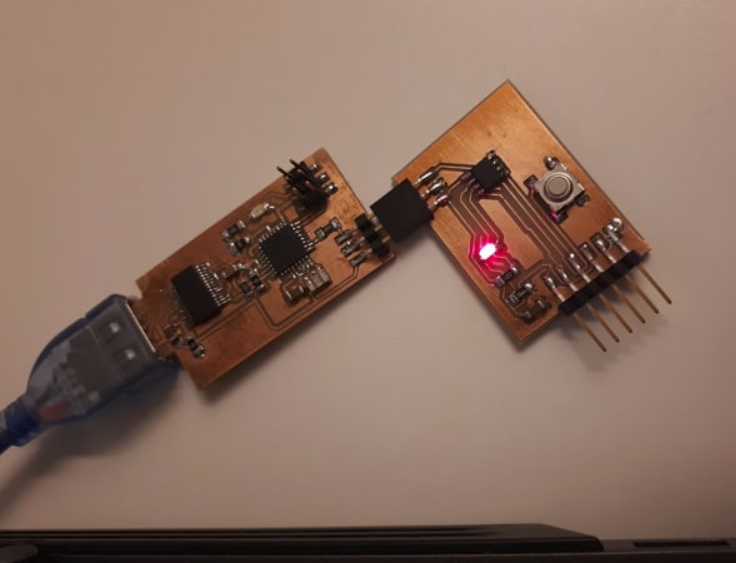
- Upload echo.ino program
- Connect the new board to the programmer
-
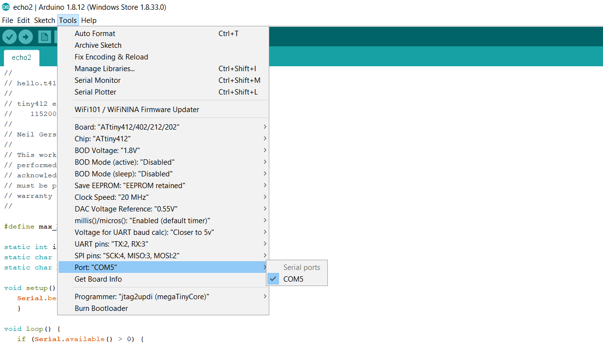
Audrino setup:
- Tools > Board: “ATtiny412/402/212/202”
- Port: [COM Port]
- Programmer:”jtag2updi(megaTinyCore)”
- Upload!
-
Connect the board to PC
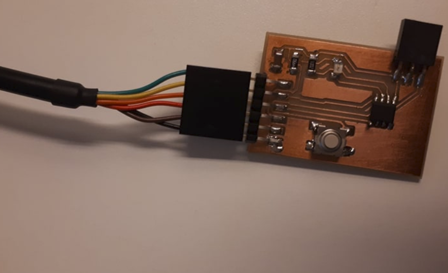
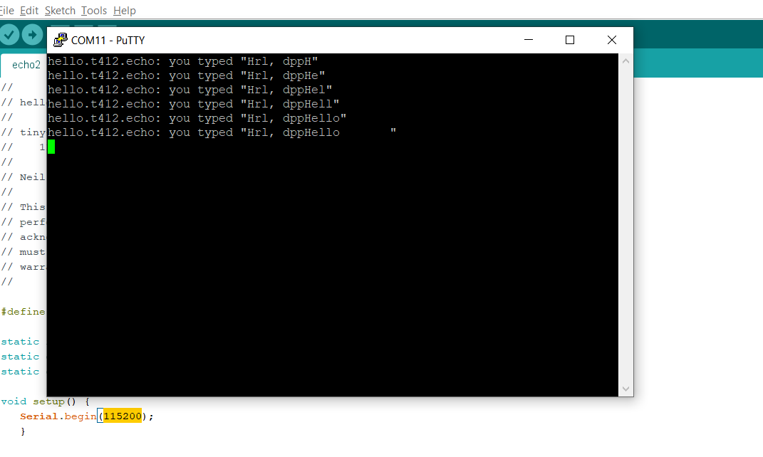
-
PuTTY setup:
- Serial Line > [COM Port]
- Speed > 115200
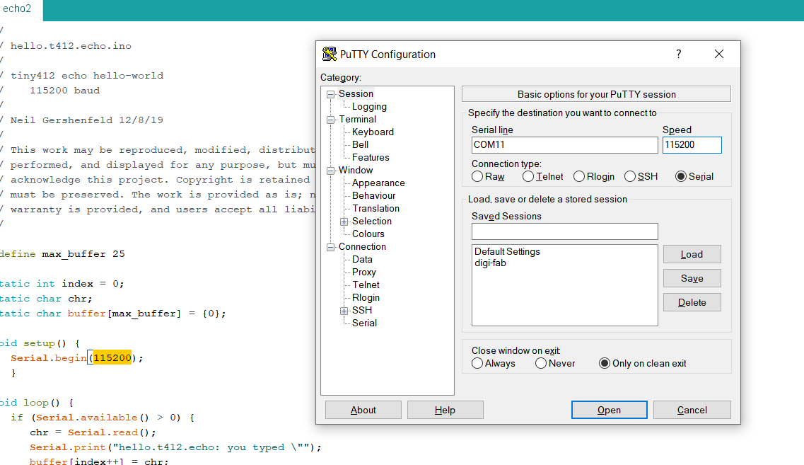
- Observe the communication interface!
Files
Eagle Schematic and Board, PNG files and .rml files
Group Work
https://fabacademy.org/2020/labs/oulu/students/zhengya-gong/assignments/week06/#group-assignment_1